TI公司的DRV8300是100V三个半桥栅极驱动器,能驱动高边和低边N沟功率MOSFET. DRV8300D能采用外接的阴极负载二极管和外接电容产生正确的栅极驱动电压,用于高边MOSFET;而DRV8300N能采用外接的阴极负载二极管和外接电容产生正确的栅极驱动电压,用于高边MOSFET. GVDD用来产生驱动低边MOSFET的栅极电压.栅极驱动架构支持峰值高达750mA源电流和1.5-A沉电流.栅极驱动电源(GVDD)为 5-20 V,MOSFET电源(SHx)支持高达100V,支持反向和非反向INLx输入,内置防止交叉导通,通过DT引脚调整死区时间(QFN封装),固定死区时间200ns插入(TSSO P封装),支持3.3V和5V逻辑输入,20V绝对最大值,传输延迟匹配值为4ns.主要用在电动自行车, 电动滑板车和电动交通,风扇,泵和伺服驱动器,BLDC马达模块和PMSM,无绳花园电动工具和割草机,无绳真空吸尘器,无人机,机器人和RC玩具,工业和后勤机器人.本文介绍了DRV8300主要特性, DRV8300D和DRV8300N简化电路图及其框图, 应用电路图, 评估模块DRV8300Dxxx-EVM主要特性和框图,电路图,材料清单和PCB设计图.
DRV8300 is 100-V three half-bridge gate drivers, capable of driving high-side and low-side N-channel power MOSFETs. The DRV8300D generates the correct gate drive voltages using an integrated bootstrap diode and external capacitor for the highside
MOSFETs. The DRV8300N generates the correct gate drive voltages using an external bootstrap diode and external capacitor for the high-side MOSFETs.
GVDD is used to generate gate drive voltage for the low-side MOSFETs. The Gate Drive architecture supports peak up to 750-mA source and 1.5-A sink currents.
The phase pins SHx is able to tolerate the significant negative voltage transients; while high side gatedriver supply BSTx and GHx is able to support to higher positive voltage transients (125-V) abs max voltage which improves robustness of the system. Small propagation delay and delay matching specifications minimize the dead-time requirement
which further improves efficiency. Undervoltage protection is provided for both low and high side through GVDD and BST undervoltage lockout.
DRV8300主要特性:
• 100-V Three Phase Half-Bridge Gate driver
– Drives N-Channel MOSFETs (NMOS)
– Gate Driver Supply (GVDD): 5-20 V
– MOSFET supply (SHx) support upto 100 V
• Integrated Bootstrap Diodes (DRV8300D devices)
• Supports Inverting and Non-Inverting INLx inputs
• Bootstrap gate drive architecture
– 750-mA source current
– 1.5-A sink current
• Supports up to 15S battery powered applications
• Low leakage current on SHx pins (<55 μA)
• Absolute maximum BSTx voltage upto 125-V
• Supports negative transients upto -22-V on SHx
• Built-in cross conduction prevention
• Adjustable deadtime through DT pin for QFN package variants
• Fixed deadtime insertion of 200 nS for TSSOP package variants
• Supports 3.3-V and 5-V logic inputs with 20 V Abs max
• 4 nS typical propogation delay matching
• Compact QFN and TSSOP packages
• Efficient system design with Power Blocks
• Integrated protection features
– BST undervoltage lockout (BSTUV)
– GVDD undervoltage (GVDDUV)
DRV8300应用:
• E-Bikes, E-Scooters, and E-Mobility
• Fans, Pumps, and Servo Drives
• Brushless-DC (BLDC) Motor Modules and PMSM
• Cordless Garden and Power Tools, Lawnmowers
• Cordless Vacuum Cleaners
• Drones, Robotics, and RC Toys
• Industrial and Logistics Robots
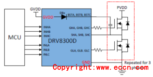
图1. DRV8300D简化电路图
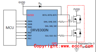
图2. DRV8300N简化电路图
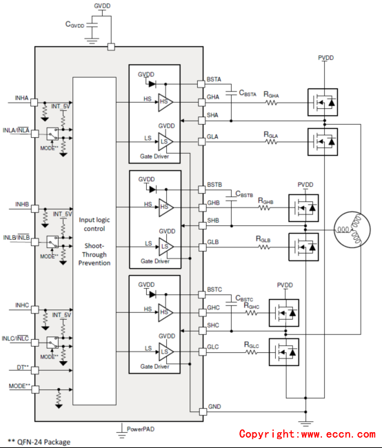
图3. DRV8300D框图
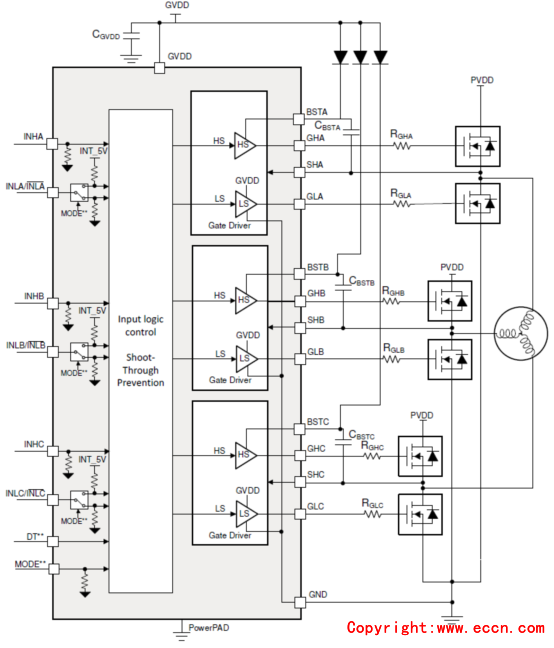
图4. DRV8300N框图
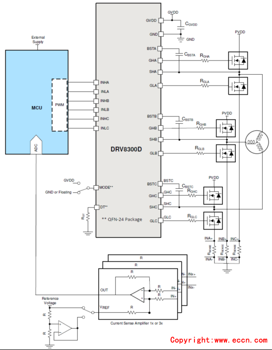
图5. DRV8300D应用电路图
The DRV8300 is a gate driver IC for three-phase motor drive applications. It provides three high-accuracy trimmed and temperature compensated half-bridge drivers, each capable of driving high-side and low-side Ntype MOSFETs.
Along with the hardware of the DRV8300, the TMS320F280049C microcontroller-based board has reference software that sends necessary signals to the DRV8300 to spin a 3-phase Brushless-DC motor. GuiComposer software allows the user to program settings, enable the motor to spin, and monitor the system from fault conditions.
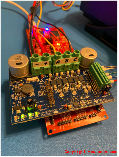
图6.评估模块DRV8300Dxxx-EVM外形图
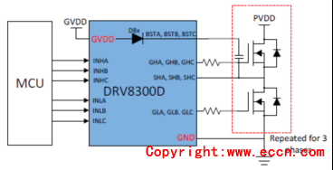
图7.评估模块DRV8300Dxxx-EVM框图
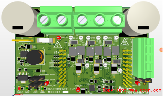
图8.评估模块DRV8300Dxxx-EVM概述框图
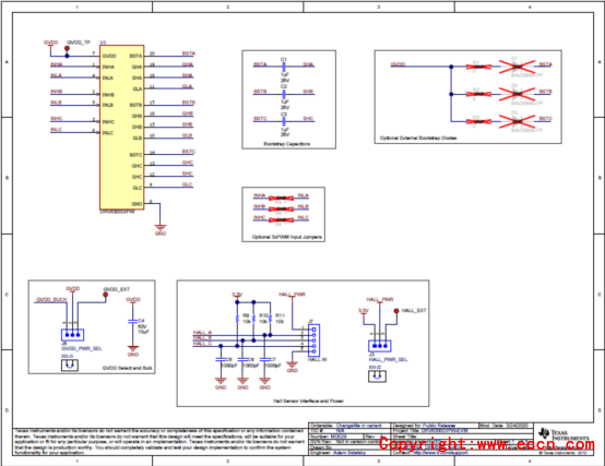
图9.评估模块DRV8300Dxxx-EVM电路图(1)
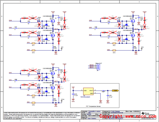
图10.评估模块DRV8300Dxxx-EVM电路图(2)
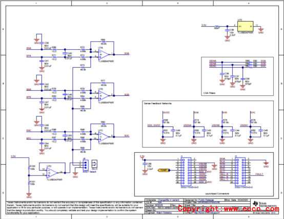
图11.评估模块DRV8300Dxxx-EVM电路图(3)
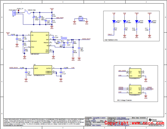
图12.评估模块DRV8300Dxxx-EVM电路图(4)
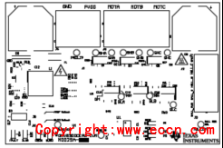
图13.评估模块DRV8300Dxxx-EVM PCB设计图(1)
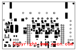
图14.评估模块DRV8300Dxxx-EVM PCB设计图(2)
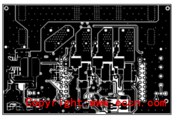
图15.评估模块DRV8300Dxxx-EVM PCB设计图(3)

图16.评估模块DRV8300Dxxx-EVM PCB设计图(4)
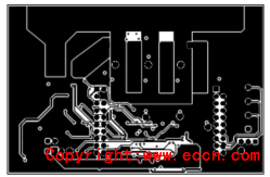
图17.评估模块DRV8300Dxxx-EVM PCB设计图(5)
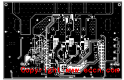
图18.评估模块DRV8300Dxxx-EVM PCB设计图(6)
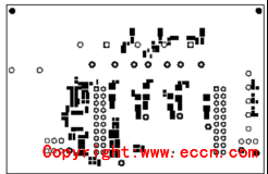
图19.评估模块DRV8300Dxxx-EVM PCB设计图(7)
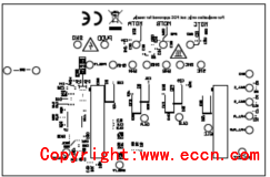
图20.评估模块DRV8300Dxxx-EVM PCB设计图(8)
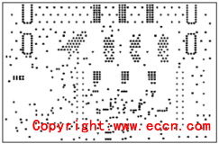
图21.评估模块DRV8300Dxxx-EVM PCB设计图(9)

图22.评估模块DRV8300Dxxx-EVM PCB设计图(10)
|
||||||||||||
|
||||||||||||


