


TI公司的TPS55288是带I2C接口同步降压/升压的压转换器,集成了两个16A MOSFET,以平衡解决方案尺寸和USB PD应用效率.TPS55288输入电压高达36V,工作在降压模式时输出电流15A.工作在升压模式是,器件8V输入时提供100W或5V输入时提供60W.开关频率通过外接电阻可编程在200kHz到2.4MHz.通过I2C接口,输出电压可在0.8V到21.26V编程,每步20mV.TPS55288具有输出过压保护,逐个周期的开关峰值电流限制和输出短路保护.基准电压精度±1% ,固定4ms软起动时间.热关断保护,4.0mmx3.5mm Hotrod™ QFN封装.主要用在USB PD,汽车充电器,坞站和工业PC. 中电网为您整理如下详细资料,本文介绍了TPS55288主要特性,功能框图和典型应用电路,以及评估模块TPS55288EVM-045快速连接图,电路图,材料清单和PCB设计图.
The TPS55288 is a synchronous buck-boostconverter optimized for converting battery voltage oradaptor voltage into power supply rails. TheTPS55288 integrates two 16-A MOSFETs of theboost leg to balance the solution size and efficiencyfor USB Power Delivery (USB PD) application.
The TPS55288 has up to 36 V input voltagecapability. It can output 15 A when working in buckmode. When working in boost mode,the devicedelivers 100 W from 8 V input or 60 W from 5 V input.When the input is a single cell Li-ion battery, thedevice outputs 45 W with input voltage down to 3.1 V.
The switching frequency is programmable from 200kHz to 2.4 MHz through an external resistor.
Through the I2C interface, the output voltage of theTPS55288 can be programmed from 0.8 V to 21.26 Vwith a 20-mV step. The default output voltage is 5 Vwhen the device is enabled.
The TPS55288 has output over-voltage protection,cycle-by-cycle switch peak-current limit, and outputshort-circuit protection.
The TPS55288 can use a small inductor and smallcapacitors with high switching frequency. It isavailable in 4.0-mm × 3.5-mm QFN package.
The TPS55288 is a 16-A buck-boost DC-to-DC converter with integrated two MOSFETs of the boost leg. TheTPS55288 can operate over a wide range of 2.7 V to 36 V input voltage and an output voltage of 0.8 V to 21.26V. It can transition among buck mode, buck-boost mode, and boost mode smoothly according to the inputvoltage and setting output. The TPS55288 operates in the buck mode when the input voltage is greater than theoutput voltage and in the boost mode when the input voltage is less than the output voltage. When the inputvoltage is close to the output voltage, the TPS55288 operates in one-cycle buck and one-cycle boost modealternately.
The TPS55288 uses an average current mode control scheme. Current mode control provides simplified loopcompensation, rapid response to the load transients and inherent line voltage rejection. An error amplifiercompares the feedback voltage of the output voltage with the internal reference voltage. The output of the erroramplifier determines the average inductor current.
An internal oscillator can be configured to operate over a wide range of frequency from 200 kHz to 2.4 MHz. Theinternal oscillator can also synchronize to an external clock applied to the DITH/SYNC pin. To minimize EMI, theTPS55288 can dither the switching frequency ranging at ±10% of the setting frequency.
The TPS55288 works in fixed-frequency PWM mode at moderate to heavy load currents. In the light loadcondition, the TPS55288 can be configured to automatically transition to PFM mode or be forced in PWM modeby either connecting a resistor at the MODE pin or setting the corresponding bit in an internal register.
User can adjust the output voltage of the device by setting the internal register through I2C interface. An internal10-bit DAC adjusts the reference voltage related to the value writing into the DAC register. The device can alsolimit the output current by placing a current sense resistor in the output path. These two functions support theprogrammable power supply (PPS) feature of the USB-PD.
The TPS55288 provides average inductor current limit set by a resistor at the ILIM pin. In addition, it providescycle-by-cycle peak inductor current limit during transient to protect the device against the current conditionbeyond the capability of the device.
A precision voltage threshold of 1.23 V with 5-μA sourcing current at the EN/UVLO pin supports programmableinput undervoltage lockout (UVLO) with hysteresis. The output over-voltage protection (OVP) feature turns off thehigh-side FETs to prevent damage to the devices powered by the TPS55288.
The device provides hiccup mode option to reduce the heating in the power components when the output shortcircuit happens. When the hiccup mode is enabled, the TPS55288 turns off for 78 ms and restarts at soft startup.
TPS55288主要特性:
• Input voltage range: 2.7 V to 36 V
• Output voltage range: 0.8 V to 21.26 V
• 97% efficiency at VIN = 12 V, VOUT = 20 V andIOUT = 3 A
• Programmable average inductor current limit up to16 A
• Adjustable switching frequency 200 kHz to2.4 MHz
• Adjustable output voltage compensation forvoltage droop over the cable
• Programmable PFM and FPWM mode at lightload
• Programmable output voltage up to 21.26 V
• Programmable output current limit
• ±1% reference voltage accuracy
• Fixed 4-ms soft-start time
• I2C Interface
• Output over-voltage protection
• Hiccup mode for output short-circuit protection
• Thermal shutdown protection
• 4.0-mm × 3.5-mm Hotrod™ QFN package
TPS55288应用:
• USB PD
• Car charger
• Docking station
• Industrial PC
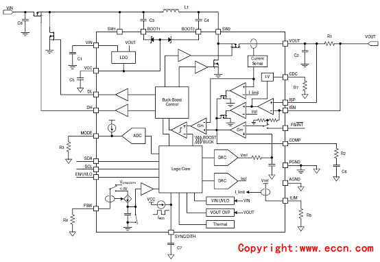
图1.TPS55288功能框图
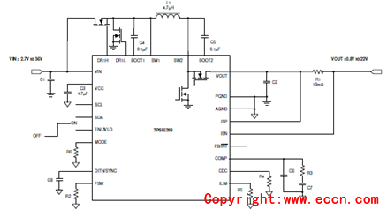
图2.TPS55288典型应用电路
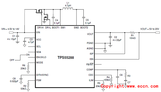
图3.TPS55288 4.5V-14V输入电压USB-PD电源电路
评估模块TPS55288EVM-045
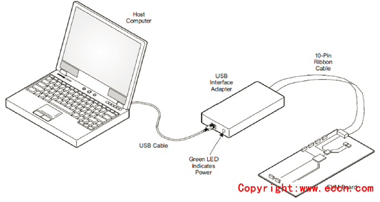
图4.评估模块TPS55288EVM-045快速连接图
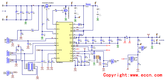
图5.评估模块TPS55288EVM-045电路图
评估模块TPS55288EVM-045材料清单:
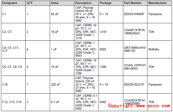
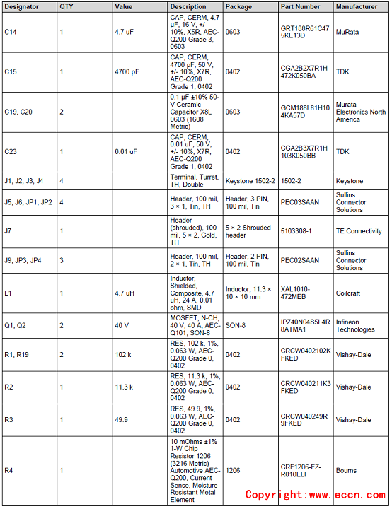
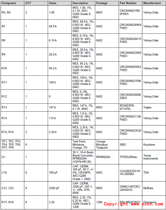
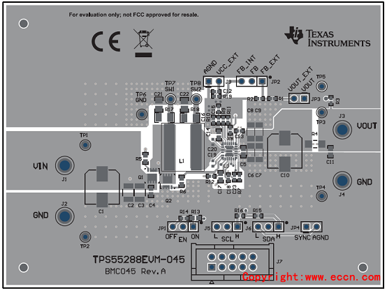
图6.评估模块TPS55288EVM-045 PCB设计图:顶层布局
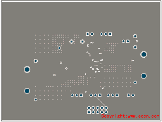
图7.评估模块TPS55288EVM-045 PCB设计图:内层1
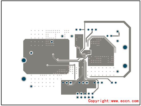
图8.评估模块TPS55288EVM-045 PCB设计图:内层2
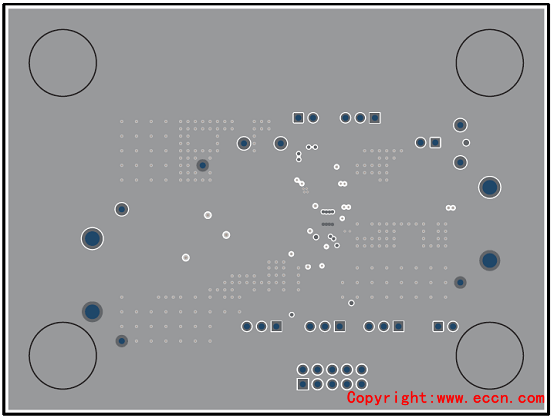
图9.评估模块TPS55288EVM-045 PCB设计图:底层布局
|
||||||||||||||||||||||||||||||
|
||||||||||||||||||||||||||||||