当前位置:首 页 --> 技术分享
INA1620高保真音频运算放大器解决方案
发布时间:2020/1/17 11:11:00 来源:永阜康科技
TI公司的INA1620是集成了精密匹配的薄膜电阻对和EMI滤波器的高保真音频运算放大器,具有低失真高输出电流两个音频运算放大器.放大器的低噪音密度为2.8-nV/√Hz,1 kHz的THD+N为-119.2dB,150mW输出功率时能驱动32-Ω负载.集成的薄膜电阻匹配度在0.004%内,可以用来创建大量的非常高性能的音频电路.INA1620工作电压±2 V 到 ±18 V,每路电流仅为2.6mA.它的关断模式使放大器的待机电流小于5 μA.放大器增益带宽为21MHz(G=+1000),转换速率为10 V/μs,电容负载驱动能力大于600 pF,600-Ω负载时的开路增益为136dB,器件的工作温度从–40℃ 到+125℃.主要用在高保真(HiFi)耳机驱动器,专业音频设备,模拟和数字混合控制台,音频测试和测量.本文介绍了INA1620主要特性,功能框图和耳机放大器应用电路,专业麦克风预放大器电路以及音频放大器评估模块INA1620 EVM主要特性,电路图,材料清单和PCB设计图.
The INA1620 integrates 4 precision-matched thin-filmresistor pairs and EMI filtering on-chip with a lowdistortion,high output current, dual audio operationalamplifier. The amplifier achieves a very low,2.8-nV/√Hz noise density with an ultra-low THD+N of–119.2 dB at 1 kHz and drives a 32-Ω load at 150-mW output power. The integrated thin-film resistorsare matched to within 0.004% and can be used tocreate a large number of very high-performanceaudio circuits.
The INA1620 operates over a very wide supply rangeof ±2 V to ±18 V on only 2.6 mA of supply current perchannel. The INA1620 also has a shutdown mode,allowing the amplifiers to be switched from normaloperation to a standby current that is typically less than 5 μA. Shutdown mode is specifically designed toeliminate click-and-pop noise when transitioning intoor out of shutdown mode.
The INA1620 has a unique internal layout for lowestcrosstalk, and freedom from interactions betweenchannels, even when overdriven or overloaded. Thisdevice is specified from –40℃ to +125℃.
The INA1620 integrates a dual, bipolar-input, audio operational amplifier with four high-precision thin-film resistorpairs on the same die. The internal amplifiers and resistor pairs are pinned out to allow for many circuitconfigurations.
The internal amplifiers of the INA1620 use a unique topology to deliver high output current with extremely lowdistortion while consuming minimal supply current. A single gain-stage architecture, combining a high-gaintransconductance input stage and a unity-gain output stage, allows the INA1620 to achieve an open-loop gain of136 dB, even with 600-Ω loads.A separate enable circuit maintains control of the input and output stage when the amplifier is placed into itsshutdown mode and limits transients at the amplifier output when transitioning to and from this state. The enablecircuit features logic levels referenced to the amplifier ground pin. This configuration simplifies the interfacebetween the amplifier and the ground-referenced GPIO pins of microcontrollers. The addition of a ground pin tothe amplifier provides several additional benefits. For example, the compensation capacitor between the inputand output stages of the INA1620 is referenced to the ground pin, greatly improving PSRR.
INA1620主要特性:
• High-Quality Thin-Film ResistorsMatched to 0.004% (Typical)
• Integrated EMI Filters
• Ultra-low Noise: 2.8 nV/√Hz at 1 kHz
• Ultra-low Total Harmonic Distortion + Noise:
–119 dB THD+N (142 mW/ChInto 32 Ω/Ch)
• Wide Gain Bandwidth Product:32 MHz (G = +1000)
• High Slew Rate: 10 V/μs
• High Capacitive-Load Drive Capability: > 600 pF
• High Open-Loop Gain: 136 dB (600-Ω Load)
• Low Quiescent Current: 2.6 mA per Channel
• Low-Power Shutdown Mode With Reduced Popand-Click Noise: 5 μA per Channel
• Short-Circuit Protection
• Wide Supply Range: ±2 V to ±18 V
• Available in Small 24-pin WQFN Package
INA1620应用:
• High-Fidelity (HiFi) Headphone Drivers
• Professional Audio Equipment
• Analog and Digital Mixing Consoles
• Audio Test and Measurement
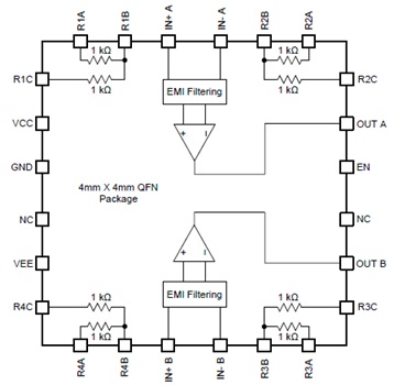
图1.INA1620功能框图
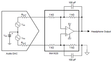
图2.INA1620应用电路:耳机放大器
耳机放大器设计要求:
• ±5-V power supplies
• 150-mW output power (32-Ω load)
• < –110-dB THD+N at maximum output (32-Ω load)
• < 0.01-dB magnitude deviation (20 Hz to 20 kHz)
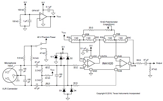
图3.专业麦克风预放大器电路
音频放大器评估模块INA1620 EVM
This user’s guide contains information for the INA1620 device as well as support documentation for theINA1620 evaluation module (EVM). Included are the performance specifications, set-up procedure,modifications, measured data, printed circuit board (PCB) layout, schematic, and bill of materials (BOM) ofthe INA1620EVM.
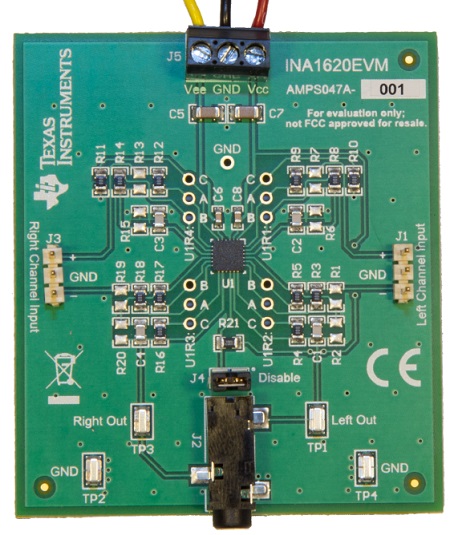
图4.音频放大器评估模块INA1620 EVM外形图
INA1620 EVM测试性能总结:

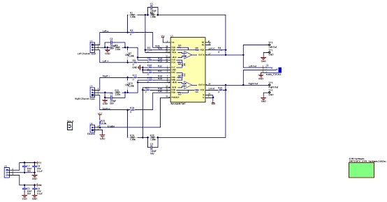
图5.INA1620 EVM电路图
INA1620 EVM材料清单:
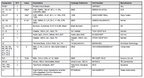
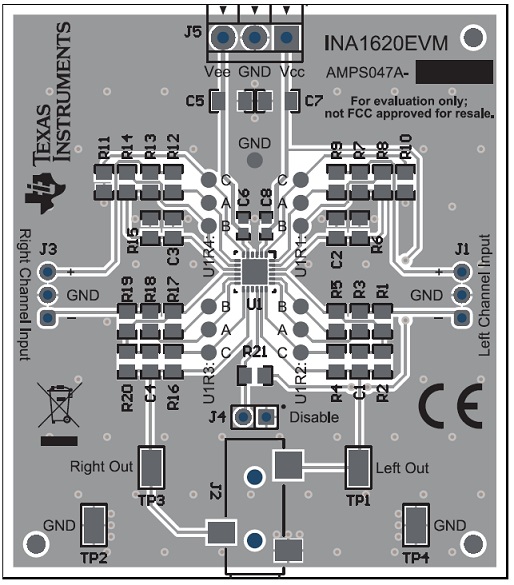
图6.INA1620 EVM PCB设计图:顶层布局
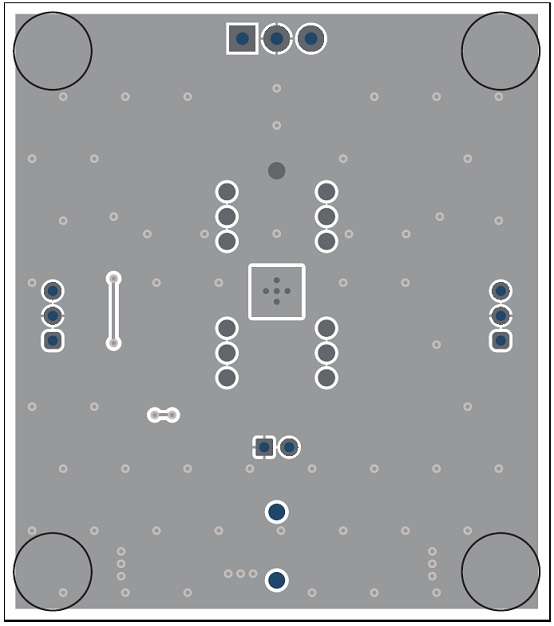
图7.INA1620 EVM PCB设计图:底层布局
The INA1620 integrates 4 precision-matched thin-filmresistor pairs and EMI filtering on-chip with a lowdistortion,high output current, dual audio operationalamplifier. The amplifier achieves a very low,2.8-nV/√Hz noise density with an ultra-low THD+N of–119.2 dB at 1 kHz and drives a 32-Ω load at 150-mW output power. The integrated thin-film resistorsare matched to within 0.004% and can be used tocreate a large number of very high-performanceaudio circuits.
The INA1620 operates over a very wide supply rangeof ±2 V to ±18 V on only 2.6 mA of supply current perchannel. The INA1620 also has a shutdown mode,allowing the amplifiers to be switched from normaloperation to a standby current that is typically less than 5 μA. Shutdown mode is specifically designed toeliminate click-and-pop noise when transitioning intoor out of shutdown mode.
The INA1620 has a unique internal layout for lowestcrosstalk, and freedom from interactions betweenchannels, even when overdriven or overloaded. Thisdevice is specified from –40℃ to +125℃.
The INA1620 integrates a dual, bipolar-input, audio operational amplifier with four high-precision thin-film resistorpairs on the same die. The internal amplifiers and resistor pairs are pinned out to allow for many circuitconfigurations.
The internal amplifiers of the INA1620 use a unique topology to deliver high output current with extremely lowdistortion while consuming minimal supply current. A single gain-stage architecture, combining a high-gaintransconductance input stage and a unity-gain output stage, allows the INA1620 to achieve an open-loop gain of136 dB, even with 600-Ω loads.A separate enable circuit maintains control of the input and output stage when the amplifier is placed into itsshutdown mode and limits transients at the amplifier output when transitioning to and from this state. The enablecircuit features logic levels referenced to the amplifier ground pin. This configuration simplifies the interfacebetween the amplifier and the ground-referenced GPIO pins of microcontrollers. The addition of a ground pin tothe amplifier provides several additional benefits. For example, the compensation capacitor between the inputand output stages of the INA1620 is referenced to the ground pin, greatly improving PSRR.
INA1620主要特性:
• High-Quality Thin-Film ResistorsMatched to 0.004% (Typical)
• Integrated EMI Filters
• Ultra-low Noise: 2.8 nV/√Hz at 1 kHz
• Ultra-low Total Harmonic Distortion + Noise:
–119 dB THD+N (142 mW/ChInto 32 Ω/Ch)
• Wide Gain Bandwidth Product:32 MHz (G = +1000)
• High Slew Rate: 10 V/μs
• High Capacitive-Load Drive Capability: > 600 pF
• High Open-Loop Gain: 136 dB (600-Ω Load)
• Low Quiescent Current: 2.6 mA per Channel
• Low-Power Shutdown Mode With Reduced Popand-Click Noise: 5 μA per Channel
• Short-Circuit Protection
• Wide Supply Range: ±2 V to ±18 V
• Available in Small 24-pin WQFN Package
INA1620应用:
• High-Fidelity (HiFi) Headphone Drivers
• Professional Audio Equipment
• Analog and Digital Mixing Consoles
• Audio Test and Measurement

图1.INA1620功能框图

图2.INA1620应用电路:耳机放大器
耳机放大器设计要求:
• ±5-V power supplies
• 150-mW output power (32-Ω load)
• < –110-dB THD+N at maximum output (32-Ω load)
• < 0.01-dB magnitude deviation (20 Hz to 20 kHz)

图3.专业麦克风预放大器电路
音频放大器评估模块INA1620 EVM
This user’s guide contains information for the INA1620 device as well as support documentation for theINA1620 evaluation module (EVM). Included are the performance specifications, set-up procedure,modifications, measured data, printed circuit board (PCB) layout, schematic, and bill of materials (BOM) ofthe INA1620EVM.

图4.音频放大器评估模块INA1620 EVM外形图
INA1620 EVM测试性能总结:


图5.INA1620 EVM电路图
INA1620 EVM材料清单:


图6.INA1620 EVM PCB设计图:顶层布局

图7.INA1620 EVM PCB设计图:底层布局
|
||||||||||||
|
||||||||||||


