当前位置:首 页 --> 方案设计
L9907三相BLDC马达驱动解决方案
发布时间:2019/4/16 9:58:00 来源:永阜康科技


ST公司的L9907是三相栅极驱动器,采用ST公司的先进的BCD-6s技术,能驱动用于3相BLDC马达的所有PowerMOS晶体管L9907满足汽车规范AEC-Q100,电源电压从4.2V到54V,用于工作在单(12V)系统,双(24V)系统和48V电池应用,在FET高边驱动器引脚上能经受住-7 V - 90 V,低待机电流功耗,PWM工作频率高达20kHz,栅极驱动器电流可通过SPI四步调整,调整范围通过外接电阻最大栅极控制电流为600mA.此外还有保护和诊断功能:FET驱动器具有电源欠压(UV)诊断,栅到源输出电压限制,栅到源无源开关断开;电源VB和VCC有过压(OV),欠压(UV)诊断和保护功能,所有逻辑引脚能经受35V,超温诊断和关断,主要用于3相栅极驱动器和汽车FET驱动器.本文介绍了L9907主要特性,框图,三相马达控制图以及评估板EVAL-L9907应用框图,主板电路图和逆变器板电路图表与PCB设计图.
L9907 is a smart power device realized in STMicroelectronics advanced BCD-6s technology. It is able to drive all PowerMOS transistors for 3-phase BLDC motor applications. The circuit is suitable to operate in environments with high supply voltage such as double battery. Supply related pins are capable of withstanding up to 90 V. Moreover, the device is able to control the six pre-driver channels independently. In this way it is possible to implement all kinds of electric motor control strategy.
The integrated boost regulator provides sufficient gate charge for all PowerMOS down to a battery voltage of 6 V. All pre-drivers have dedicated connections with the MOSFET sources. The device offers programmability for a base gate output current via an external resistor. Moreover, via SPI, it is possible to select among 4 gate output current levels even while the application is running. All channels are protected against short circuit and the device is protected against overtemperature conditions. Moreover, the boost converter implements an over voltage protection to allow safe functionality of pre-drivers in all battery voltage conditions. During over voltage conditions, BST_C voltage is limited by temporarily switching off the boost regulator and pre-drivers are allowed to operate. Boost will be self re-enabled as soon as the output voltage decreases to an acceptable value.
The device is equipped with 2 current sense amplifiers. Both have SPI selectable amplifier gain (10, 30, 50 and 100) and output offset voltage level in order to allow max flexibility for phase or ground current sense strategy. All I/O pins are 35 V compatible. Full diagnostic is available through SPI. The device is available in TQFP64 and bare die, depending on the application requirements.The device is protected against Shoot Through events.
L9907主要特性:
AEC-Q100 qualified
Supply voltage from 4.2V to 54 V for working in single (12 V systems), double (24 V systems) and 48 V battery applications
The device can withstand -7 V to 90 V at the FET high-side Driver pins
Low standby current consumption
3.3 V internal regulator supplied by Vcc pin
Boost regulator for full Rdson down to 6 V and over voltage protection
3 low-side + 3 high-side drivers
– PWM operation up to 20 kHz
– Gate driver current adjustable via SPI in 4 steps. Range set via external resistor. Maximum gate controlled current 600 mA
– Source connection to each MOSFET
Input pin for each gate driver
2-differential current sense amplifiers:
– Output offset selectable via SPI (0.2*Vcc offset for ground shunt resistors connection, 0.5*Vcc offset for phase shunt resistors connection)
– All the amplifier gain factors are programmable (10, 30, 50, 100)
8 MHz, 16-bit SPI
Full diagnostic
Programmable parameters:
– Cross conduction dead time with a fixed minimum value
– 4 current steps driving the PowerMOS gates (25%, 50%, 75%, 100%)
– Phase or ground selection of current sense amplifier
– Gain values for the current sense amplifiers
– Zero current output voltage (offset) for the current sense amplifiers
– Over voltage threshold selection for single or double battery operation
– Short circuit detection thresholds for the low-side and the high-side MOSFETs (drain to source voltage monitor).
Protection and diagnostic
FET driver:
– FET driver supply Undervoltage (UV) diagnostic;
– Gate to source output voltage limit;
– Gate to source passive switch off.
Power supply pins VB and VCC:
– Overvoltage (OV), Undervoltage (UV) diagnostic and protection
All logic pins withstand 35 V
Power MOSFET drain to source voltage drop measurement for overcurrent protection Over-temperature diagnostic and shutdown
Fault status flag output
图1.L9907框图
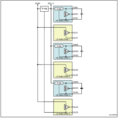
图2.MOSFET驱动器电源架构图
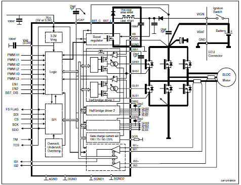
图3.三相马达控制图
评估板EVAL-L9907
The EVAL-L9907 is an evaluation board designed to provide the user a platform for the L9907, a FET driver for 3 phase BLDC motor. The board offers all the main input/output capabilities needed to drive a BLCD motor properly and to provide diagnostic functionalities.
Full diagnostic is available through SPI. By using SPI communication, it is possible to program L9907 while the application is running (e.i. set the gain of the current sense amplifier).
A dedicated pin array allows connecting easily a SPC5 discovery+ board and the EVAL-L9907. In association with the discovery board SPC560P-DISP a dedicated SW allows controlling a motor control application by using a PC via a USB port.
L9907 device is able to control the six pre-driver channels independently and all pre-drivers have dedicated connections with the output MOSFETs; this feature gives the user the possibility to implement all kinds of electric motor control strategy. All gate driver outputs are protected against short circuit and L9907 is protected against over-temperature condition.
Three terminal blocks are dedicated to connect the three wires of a BLDC Motor (3-phases), moreover, specific connectors are present to connect the feedback signals from the motor to the gate driver and to the microcontroller.
The EVAL-L9907 is an evaluation board designed to allow the whole hardware configuration flexibility, giving the user total access to all pins of the L9907.
Standard connectors connect the gate driver board (L9907) and Inverter Power MOSFET output stage; this solution allows simplifying the evaluation procedure and it increases the flexibility of the HW environment.
The main features are: Total accessibility to all device pins (both L9907 and the Inverter MOSFET board).Two separated boards: gate driver with L9007 and Inverter Power MOSFET boards with the MOSFET array. This HW architecture allows the user to evaluate the application with different HW configurations. Output power board current capability up to 20A.Full HW compatibility with the SPC56 discovery boards through the standard SPC56 Discovery+ connector, 0.1” - 4x36 pin.Possibility to connect generic microcontroller boards(a) by using a customized adapter.
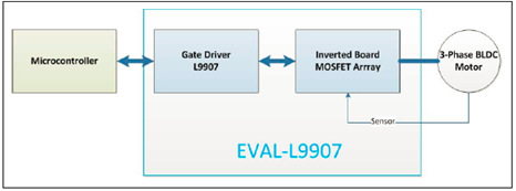
图4.评估板EVAL-L9907应用框图
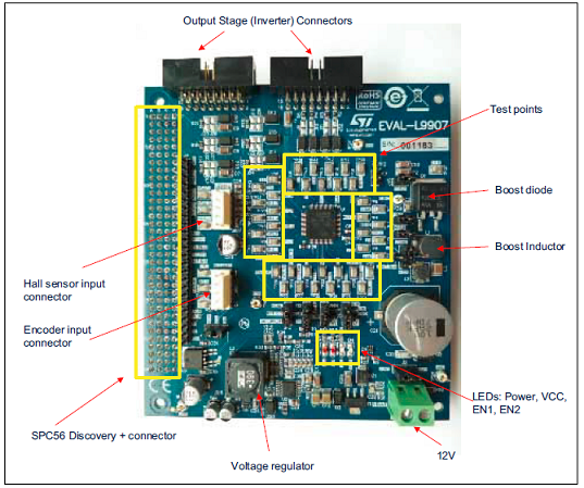
图5.L9907栅极驱动器板-元件和连接器-顶层

图6.L9907栅极驱动器板-元件和连接器-底层
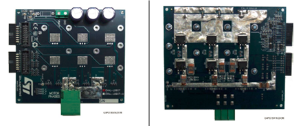
图7.L9907输出电源板外形图-顶层图8.L9907输出电源板外形图-底层
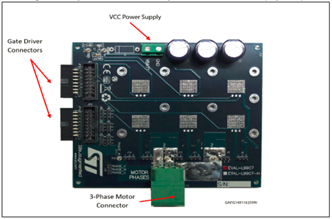
图9.L9907输出电源板-元件和连接器-顶层
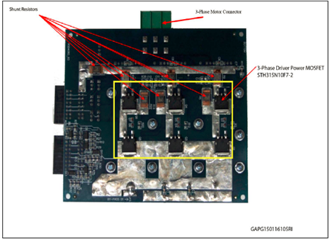
图10.L9907输出电源板-元件和连接器-底层
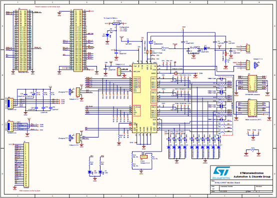
图11.评估板EVAL-L9907主板电路图(1)
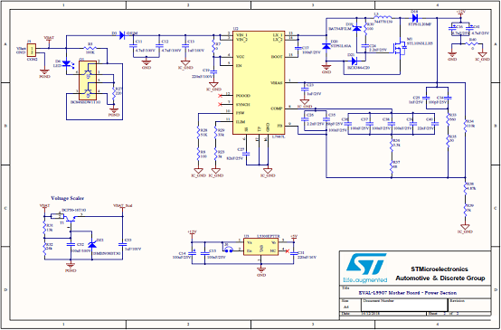
图12.评估板EVAL-L9907主板电路图(2)
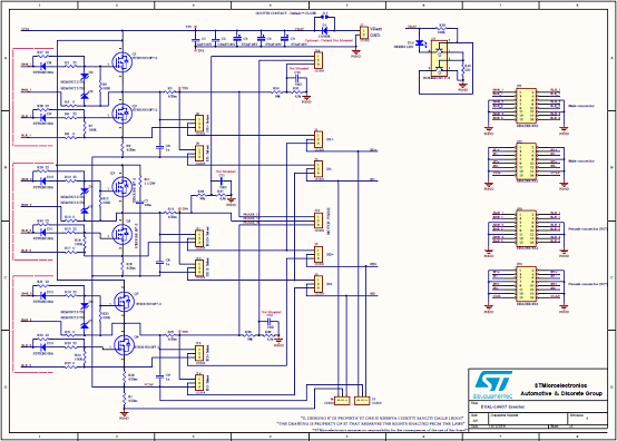
图13.评估板EVAL-L9907逆变器板电路图
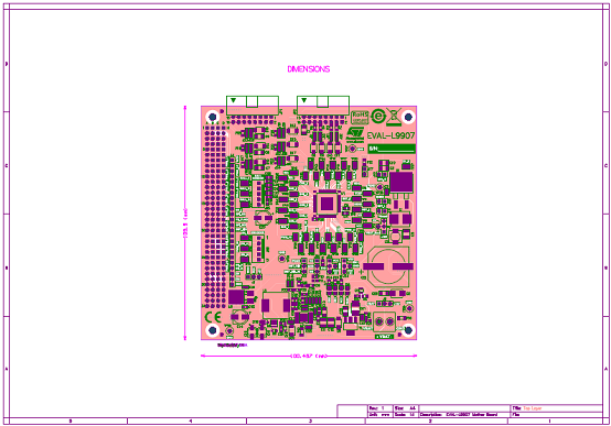
图14.评估板EVAL-L9907主板PCB设计图(1)
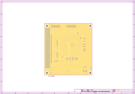
图15.评估板EVAL-L9907主板PCB设计图(2)
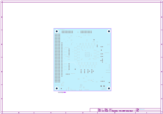
图16.评估板EVAL-L9907主板PCB设计图(3)
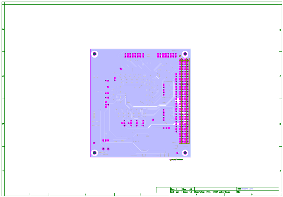
图17.评估板EVAL-L9907主板PCB设计图(4)
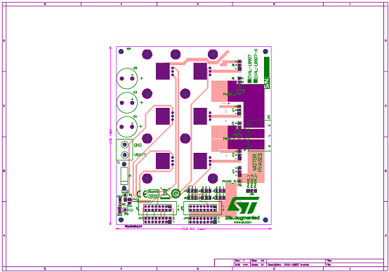
图18.评估板EVAL-L9907逆变器板PCB设计图(1)
图19.评估板EVAL-L9907逆变器板PCB设计图(2)

图20.评估板EVAL-L9907逆变器板PCB设计图(3)
图21.评估板EVAL-L9907逆变器板PCB设计图(4)
图22.评估板EVAL-L9907栅极驱动器板PCB布局图-顶层
图23.评估板EVAL-L9907栅极驱动器板PCB布局图-底层
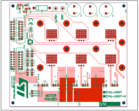
图24.评估板EVAL-L9907逆变器板PCB布局图-顶层
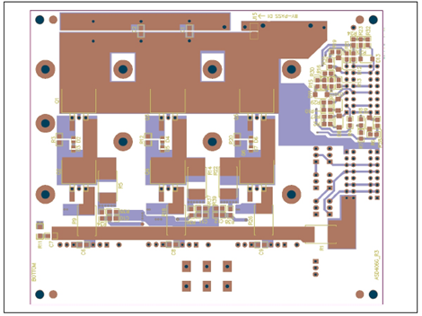
图25.评估板EVAL-L9907栅极驱动器板PCB布局图-底层
L9907 is a smart power device realized in STMicroelectronics advanced BCD-6s technology. It is able to drive all PowerMOS transistors for 3-phase BLDC motor applications. The circuit is suitable to operate in environments with high supply voltage such as double battery. Supply related pins are capable of withstanding up to 90 V. Moreover, the device is able to control the six pre-driver channels independently. In this way it is possible to implement all kinds of electric motor control strategy.
The integrated boost regulator provides sufficient gate charge for all PowerMOS down to a battery voltage of 6 V. All pre-drivers have dedicated connections with the MOSFET sources. The device offers programmability for a base gate output current via an external resistor. Moreover, via SPI, it is possible to select among 4 gate output current levels even while the application is running. All channels are protected against short circuit and the device is protected against overtemperature conditions. Moreover, the boost converter implements an over voltage protection to allow safe functionality of pre-drivers in all battery voltage conditions. During over voltage conditions, BST_C voltage is limited by temporarily switching off the boost regulator and pre-drivers are allowed to operate. Boost will be self re-enabled as soon as the output voltage decreases to an acceptable value.
The device is equipped with 2 current sense amplifiers. Both have SPI selectable amplifier gain (10, 30, 50 and 100) and output offset voltage level in order to allow max flexibility for phase or ground current sense strategy. All I/O pins are 35 V compatible. Full diagnostic is available through SPI. The device is available in TQFP64 and bare die, depending on the application requirements.The device is protected against Shoot Through events.
L9907主要特性:
AEC-Q100 qualified
Supply voltage from 4.2V to 54 V for working in single (12 V systems), double (24 V systems) and 48 V battery applications
The device can withstand -7 V to 90 V at the FET high-side Driver pins
Low standby current consumption
3.3 V internal regulator supplied by Vcc pin
Boost regulator for full Rdson down to 6 V and over voltage protection
3 low-side + 3 high-side drivers
– PWM operation up to 20 kHz
– Gate driver current adjustable via SPI in 4 steps. Range set via external resistor. Maximum gate controlled current 600 mA
– Source connection to each MOSFET
Input pin for each gate driver
2-differential current sense amplifiers:
– Output offset selectable via SPI (0.2*Vcc offset for ground shunt resistors connection, 0.5*Vcc offset for phase shunt resistors connection)
– All the amplifier gain factors are programmable (10, 30, 50, 100)
8 MHz, 16-bit SPI
Full diagnostic
Programmable parameters:
– Cross conduction dead time with a fixed minimum value
– 4 current steps driving the PowerMOS gates (25%, 50%, 75%, 100%)
– Phase or ground selection of current sense amplifier
– Gain values for the current sense amplifiers
– Zero current output voltage (offset) for the current sense amplifiers
– Over voltage threshold selection for single or double battery operation
– Short circuit detection thresholds for the low-side and the high-side MOSFETs (drain to source voltage monitor).
Protection and diagnostic
FET driver:
– FET driver supply Undervoltage (UV) diagnostic;
– Gate to source output voltage limit;
– Gate to source passive switch off.
Power supply pins VB and VCC:
– Overvoltage (OV), Undervoltage (UV) diagnostic and protection
All logic pins withstand 35 V
Power MOSFET drain to source voltage drop measurement for overcurrent protection Over-temperature diagnostic and shutdown
Fault status flag output
图1.L9907框图
图2.MOSFET驱动器电源架构图
图3.三相马达控制图
评估板EVAL-L9907
The EVAL-L9907 is an evaluation board designed to provide the user a platform for the L9907, a FET driver for 3 phase BLDC motor. The board offers all the main input/output capabilities needed to drive a BLCD motor properly and to provide diagnostic functionalities.
Full diagnostic is available through SPI. By using SPI communication, it is possible to program L9907 while the application is running (e.i. set the gain of the current sense amplifier).
A dedicated pin array allows connecting easily a SPC5 discovery+ board and the EVAL-L9907. In association with the discovery board SPC560P-DISP a dedicated SW allows controlling a motor control application by using a PC via a USB port.
L9907 device is able to control the six pre-driver channels independently and all pre-drivers have dedicated connections with the output MOSFETs; this feature gives the user the possibility to implement all kinds of electric motor control strategy. All gate driver outputs are protected against short circuit and L9907 is protected against over-temperature condition.
Three terminal blocks are dedicated to connect the three wires of a BLDC Motor (3-phases), moreover, specific connectors are present to connect the feedback signals from the motor to the gate driver and to the microcontroller.
The EVAL-L9907 is an evaluation board designed to allow the whole hardware configuration flexibility, giving the user total access to all pins of the L9907.
Standard connectors connect the gate driver board (L9907) and Inverter Power MOSFET output stage; this solution allows simplifying the evaluation procedure and it increases the flexibility of the HW environment.
The main features are: Total accessibility to all device pins (both L9907 and the Inverter MOSFET board).Two separated boards: gate driver with L9007 and Inverter Power MOSFET boards with the MOSFET array. This HW architecture allows the user to evaluate the application with different HW configurations. Output power board current capability up to 20A.Full HW compatibility with the SPC56 discovery boards through the standard SPC56 Discovery+ connector, 0.1” - 4x36 pin.Possibility to connect generic microcontroller boards(a) by using a customized adapter.
图4.评估板EVAL-L9907应用框图
图5.L9907栅极驱动器板-元件和连接器-顶层
图6.L9907栅极驱动器板-元件和连接器-底层
图7.L9907输出电源板外形图-顶层图8.L9907输出电源板外形图-底层
图9.L9907输出电源板-元件和连接器-顶层
图10.L9907输出电源板-元件和连接器-底层
图11.评估板EVAL-L9907主板电路图(1)
图12.评估板EVAL-L9907主板电路图(2)
图13.评估板EVAL-L9907逆变器板电路图
图14.评估板EVAL-L9907主板PCB设计图(1)
图15.评估板EVAL-L9907主板PCB设计图(2)
图16.评估板EVAL-L9907主板PCB设计图(3)
图17.评估板EVAL-L9907主板PCB设计图(4)
图18.评估板EVAL-L9907逆变器板PCB设计图(1)
图19.评估板EVAL-L9907逆变器板PCB设计图(2)
图20.评估板EVAL-L9907逆变器板PCB设计图(3)
图21.评估板EVAL-L9907逆变器板PCB设计图(4)
图22.评估板EVAL-L9907栅极驱动器板PCB布局图-顶层
图23.评估板EVAL-L9907栅极驱动器板PCB布局图-底层
图24.评估板EVAL-L9907逆变器板PCB布局图-顶层
图25.评估板EVAL-L9907栅极驱动器板PCB布局图-底层
|
||||||||||||
|
||||||||||||