TLE9879汽车三相马达驱动解决方案
发布时间:2019/2/23 10:46:00 来源:永阜康科技
infineon公司的TLE9879QXA20是集成了ARM® Cortex®-M3 MCU和LIN和BLDC MOSFET驱动器的三相马达驱动器,包括了全集成的NFET驱动器,它通过六个外接功率NFET来驱动3相马达;能低压工作的电荷泵以及具有电流斜率控制的可编程电流,从而最优化EMI性能.外设包括电流传感器,逐次逼近式模拟转换器(ADC)以及用于PWM控制的捕获和比较和16位计时器.此外还集成了LIN收发器和大量的通用I/O与线性稳压器以给外接负载供电.主要用在汽车燃料泵,HVAC风机,引擎冷却风扇,水泵,BLDC泵和风扇,无传感器和有传感器BLDC马达.本文介绍了TLE9879QXA20主要特性,框图以及功率管理单元框图,系统控制单元-数字模块框图,Cortex-M3核框图,简化应用框图和外接元件表,评估板TLE9879 EvalKit V1.2主要特性,电路图和PCB设计图.
The TLE9879QXA20 is part of the TLE987x product family. The TLE9879QXA20 is a single chip 3-Phase motor driver that integrates the industry standard ARM® Cortex™ M3 core, enabling the implementation of advanced motor control algorithms such as field-oriented control. It includes six fully integrated NFET drivers optimized to drive a 3-Phase motor via six external power NFETs, a charge pump enabling low voltage operation and programmable current along with current slope control for optimized EMC behavior. Its peripheral set includes a current sensor, a successive approximation ADC synchronized with the capture and compare unit for PWM control and 16-bit timers. A LIN transceiver is also integrated to enable communication to the device along with a number of general purpose I/Os. It includes an on-chip linear voltage regulator to supply external loads.
It is a highly integrated automotive qualified device enabling cost and space efficient solutions for mechatronic BLDC motor drive applications such as pumps and fans.
TLE9879QXA20主要特性:
• 32 bit ARM Cortex M3 Core
– up to 24 MHz clock frequency
– one clock per machine cycle architecture
• On-chip memory
– 128 kByteFlash including
– 4 kByte EEPROM (emulated in Flash)
– 512 Byte 100 Time Programmable Memory (100TP)
– 6 kByte RAM
– Boot ROM for startup firmware and Flash routines
• On-chip OSC and PLL for clock generation
– PLL loss-of-lock detection
• MOSFET driver including charge pump
• 10 general-purpose I/O Ports (GPIO)
• 5 analog inputs, 10-bit A/D Converter (ADC1)
• 16-bit timers - GPT12, Timer 2, Timer 21 and Timer 3
• Capture/compare unit for PWM signal generation (CCU6)
• 2 full duplex serial interfaces (UART) with LIN support (for UART1 only)
• 2 synchronous serial channels (SSC)
• On-chip debug support via 2-wire SWD
• 1 LIN 2.2 transceiver
• 1 high voltage monitoring input
• Single power supply from 5.5 V to 27 V
• Extended power supply voltage range from 3 V to 28 V
• Low-dropout voltage regulators (LDO)
• High speed operational amplifier for motor current sensing via shunt
• 5 V voltage supply for external loads (e.g. Hall sensor)
• Core logic supply at 1.5 V
• Programmable window watchdog (WDT1) with independent on-chip clock source
• Power saving modes
– MCU slow-down Mode
– Sleep Mode
– Stop Mode
– Cyclic wake-up Sleep Mode
• Power-on and undervoltage/brownout reset generator
• Overtemperature protection
• Short circuit protection
• Loss of clock detection with fail safe mode entry for low system power consumption
• Temperature Range Tj = -40℃ to +150℃
• Package VQFN-48 with LTI feature
• Green package (RoHS compliant)
• AEC qualified
TLE9879QXA20目标应用:
Fuel pump
HVAC blower
Engine cooling fan
Water pumps
BLDC pumps and fans
Sensor-less and sensor-based BLDC motor applications controlled by the Local Interconnect Network (LIN) or PWM
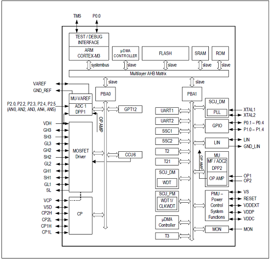
图1.TLE9879QXA20框图
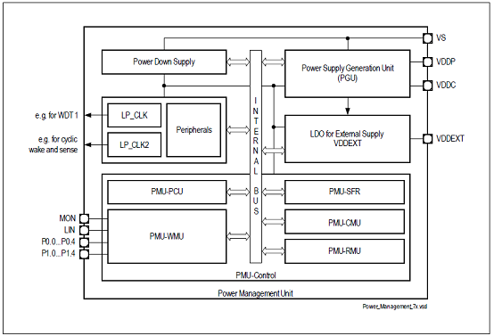
图2.TLE9879QXA20功率管理单元框图
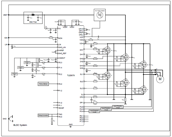
图3.TLE9879QXA20系统控制单元-数字模块框图
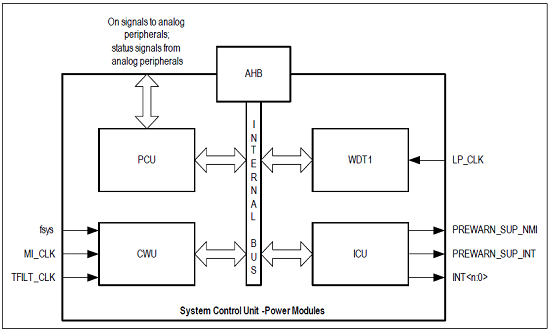
图4.TLE9879QXA20系统控制单元-功率模块框图
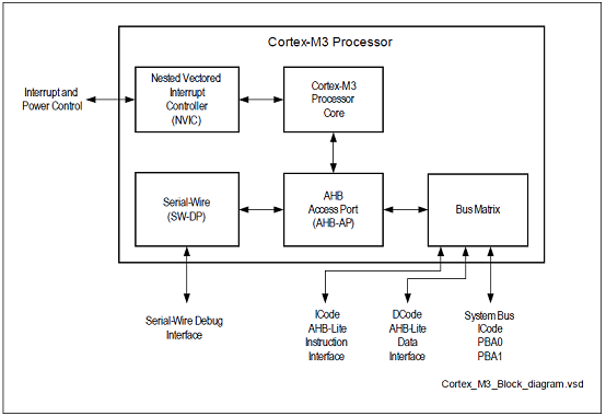
图5.TLE9879QXA20 Cortex-M3核框图

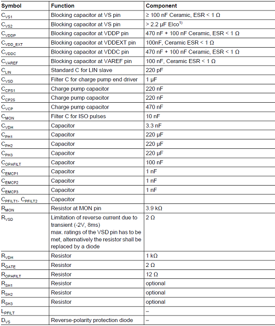
图6.TLE9879QXA20简化应用框图
图6应用框图外接元件表:
评估板TLE9879 EvalKit V1.2
This board is intended to provide a simple, easy-to-use tool for getting familiar with Infineon’s embedded power IC TLE9879. It contains the TLE9879 and its typical application circuit including three MOSFET half bridges to instantly drive a BLDC motor. The board is ready to connect with car supply or similar and has an implemented Segger for debugging on board.
All relevant chip pins are connected to pin headers at the edge of the board, where signals can be probed or applied directly. By different jumper settings LEDs can be put in parallel to several ports and selected functions can be configured. Push button switches allow easy hardware reset and triggering of the MON input. There are intended test points for all six gate driver pins, for measurements at the shunt, VDDC and several ground points on the evaluation board (see Figure 3). For testing analog signals ADC inputs can be varied by the potentiometer on board. Three phases of motor current can be picked off at a terminal block to connect a DC brushless motor.
The evaluation board can be operated by standard laboratory equipment as power supply and LIN communication are working via banana jacks. Debugging and UART are provided via an USB interface combined with onboard Segger J-Link (XMC4200). Bidirectional level shifters ensure that the respective XMC pins are in tristate as long as UART or debugging is not used.
In case the user wants to use another ISP than the onboard Segger the SWD interface can be used. To program the TLE9879 via LIN there is an additional uIO BSL interface.
There is a battery LED that indicates that the board is connected to supply the right way. Otherwise reverse polarity protection secures the board from damage by cross connection.
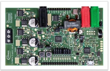
图7.评估板TLE9879 EvalKit V1.2外形图
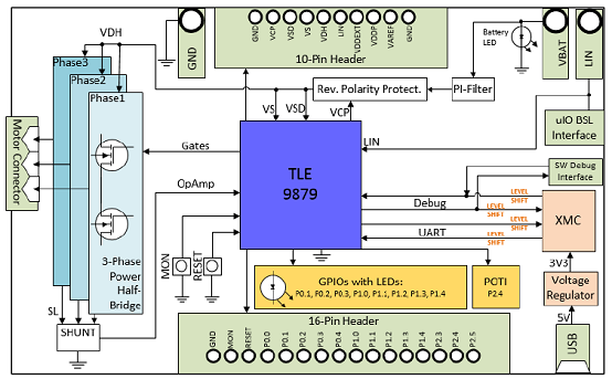
图8.评估板TLE9879 EvalKit V1.2框图
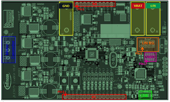
图9.评估板TLE9879 EvalKit V1.2连接图
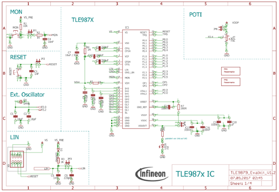
图10.评估板TLE9879 EvalKit V1.2电路图(1)
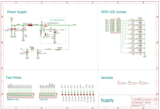
图11.评估板TLE9879 EvalKit V1.2电路图(2)
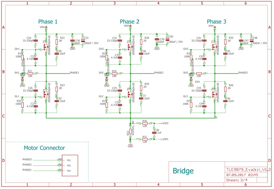
图12.评估板TLE9879 EvalKit V1.2电路图(3)
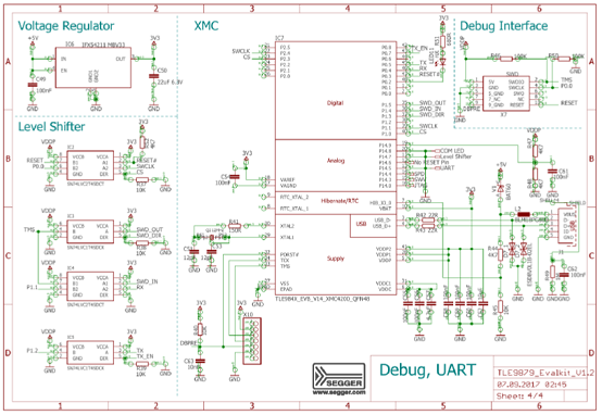
图13.评估板TLE9879 EvalKit V1.2电路图(4)
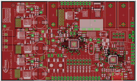
图14.评估板TLE9879 EvalKit V1.2 PCB设计图(1):顶层
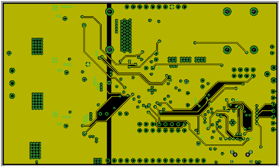
图15.评估板TLE9879 EvalKit V1.2 PCB设计图(2):层2
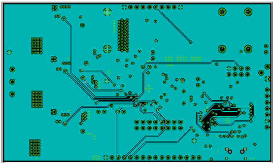
图16.评估板TLE9879 EvalKit V1.2 PCB设计图(3):层3
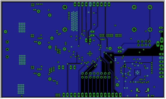
图17.评估板TLE9879 EvalKit V1.2 PCB设计图(4):底层
| |
| |
 |
您可能对以下产品感兴趣 |
 |
|
 |
| 产品型号 |
功能介绍 |
兼容型号 |
封装形式 |
工作电压 |
备注 |
| AT4931 |
AT4931 是一款三相无刷直流电机预驱动芯片,能够在宽电
压范围内驱动N 沟道功率MOSFET,且电机电源最高可支持到
30V. |
A4931 |
QFN-28 |
8V-38V |
三相直流电动机预驱动器 |
|
| |