当前位置:首 页 --> 方案设计
STHV800超声波图像系统解决方案
发布时间:2015/10/31 9:48:00 来源:
ST公司的STHV800是大容量超声波发送器,每路有两个独立的半桥,输出电压0- ±90 V,输出电流±2 A,由外部时钟可同步输入信号,工作频率高达20MHz,主要用在医用超声波图像,脉冲波形发生器,NDT超声波发送,压电变送器驱动等.本文介绍了超声波系统框图,STHV800主要特性,内部框图,评估板STEVAL-IME009V1主要特性,硬件框图,电路图和材料清单.
Remarkable advances are taking place in medical imaging. Ultrasound imaging helps examine anatomical activity within patients. ST provides with a very wide portfolio of products from discretes to 32 bit digital processors and memories that help to further enhance imaging within ultrasound imaging equipments. The block diagram facilitates your selection among a wide selection of recommended applicable products.

图1.超声波系统框图
The STHV800 is an octal, monolithic, high-voltage and high-speed pulse generator. It is designed for medical ultrasound applications, but can be used for other piezoelectric, capacitive or MEMS transducers.
The device integrates a controller logic interface circuit (compatible with both 1.8 V and 3.3 V input signals), level translators, MOSFET gate drivers, noise blocking diodes, and high power P-channel and N-channel MOSFETs as the output stage for each channel. These MOSFETs are capable of providing more than 2 A of peak output current. Each channel has a dedicated bridge in order to reduce power dissipation and jitter during continuous wave mode (peak current is limited to 0.3 A). This CW bridge has dedicated power supplies (HV_CW) which are fully independent on the main HV supplies.
These HV_CW supplies can be shorted to the HV supplies. The fundamental structure of each channel also consists of active clamping to ground circuitry, anti-leakage and anti-memory block, a thermal sensor to protect the device and an integrated TR-switch (just 8 Ω as equivalent resistor ) to connect the HV output to its LV output, guaranteeing strong decoupling during the transmission phase.
The eight independent T/R switches can be used in both a dedicated RX chain per channel or in a multiplexing configuration.
The clamp circuit has a current capability up to 2 A and works directly on the output pin, carrying this node exactly to zero. This feature allows minimized injection change during the transition from clamp to RX state.
In addition, the STHV800 includes self-biasing circuitry which allows very low power consumption during the RX phase (down to 200 μW global power dissipation) and thermal shutdown block sensing by an external dedicated pin (THSD).
One of the main benefits of this device is that it requires very few external components: only decoupling capacitors on the HV and LV supplies, and a resistor to pull up the THSD pin (moreover, this resistor can be shared by many devices).
Each channel is driven independently by only 2 digital bits, which in CW mode become one bit. An external clock can be used with the STHV800 to synchronize all the input signals. This feature, however, is optional: if the CK pin is tied to ground the device works in asynchronous mode.
STHV800主要特性:
• High-density ultrasound transmitter
• Two independent half-bridges per channel
• 0 to ±90 V output voltage
• Power-up free
• Synchronization of the input signals (selectable) by an external clock
• Up to 20 MHz operating frequency
• Low-power, high-voltage, high-speed drivers
• 2 independently-supplied half bridges (shorted-option) for each channel, one dedicated to continuous wave (CW) mode − Main half bridge: − ±2 A source and sink current
− Down to 20 ps jitter
− Low 2nd harmonic distortion
− CW half bridge: − ±0.3 A source and sink current
− Down to 10 ps jitter
− Very low power consumption
• Fully integrated real clamping-to-ground function − 8 Ω synchronous active clamp
− ±2 A source and sink current
• Fully integrated TR switch − 8 Ω ON resistance
− Up to 300 MHz BW
− Current consumption down to 10 μA in RX phase
− Receiver multiplexing function
• 1.8 V to 3.6 V CMOS logic interface
• Auxiliary integrated circuits − Noise blocking diodes
− Anti-leakage on output node
− Fully self-biasing architecture
− Thermal protection
• Latch-up free due to HV SOI technology
• Very few external passive components or supplies needed
STHV800应用:
• Medical ultrasound imaging
• Pulse waveform generator
• NDT ultrsound transmission
• Piezoelectric transducer drivers
• Point-of-care ultrasound imaging equipment
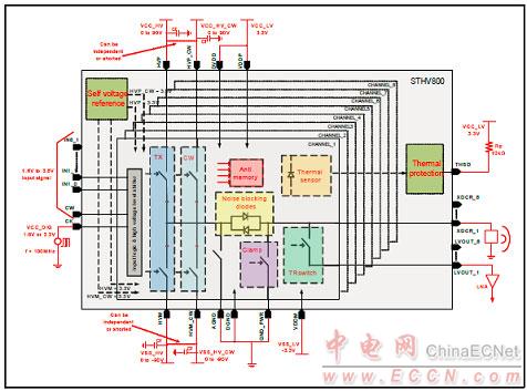
图2.STHV800内部框图
评估板STEVAL-IME009V1
The STEVAL-IME009V1 is a product evaluation board designed around the STHV800 8-channel high voltage pulser, a state-of-the-art device designed for ultrasound imaging applications.
The output waveforms can be displayed directly on an oscilloscope by connecting the scope probe to the relative BNCs. 16 preset waveforms are available to test the HV pulser under varying conditions.
评估板STEVAL-IME009V1主要特性:
8-channel outputs: high voltage and low voltage BNC connectors
Load simulator using signal equivalent circuits
Possibility to set up own load simulator
16 preset waveforms
USB connector to connect STM32 with PC and supply power to it
4 MB serial Flash memory to host FPGA code and waveforms
Memory expansion connector to add external serial Flash
Connectors to supply high voltage and low voltage to the STHV800 output stage
LEDs to monitor the power management stage
Human machine interface to select, start and stop the generation of the preset waveforms
25 LEDs to monitor board behavior
RoHS compliant
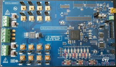
图3.评估板STEVAL-IME009V1外形图
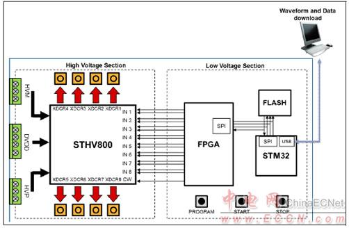
图4.评估板STEVAL-IME009V1硬件框图

图5.评估板STEVAL-IME009V1电路图(1)

图6.评估板STEVAL-IME009V1电路图(2)
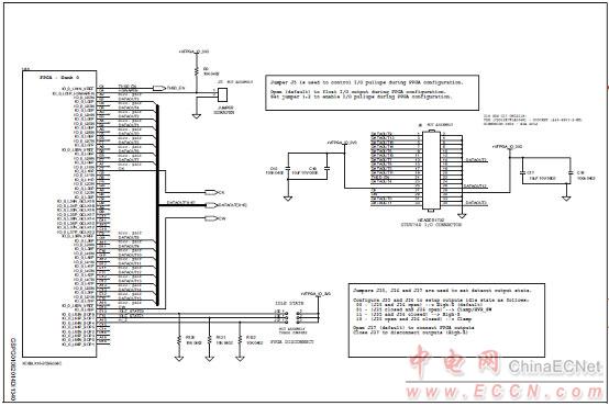
图7.评估板STEVAL-IME009V1电路图(3)

图8.评估板STEVAL-IME009V1电路图(4)

图9.评估板STEVAL-IME009V1电路图(5)

图10.评估板STEVAL-IME009V1电路图(6)
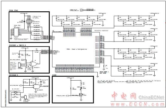
图11.评估板STEVAL-IME009V1电路图(7)
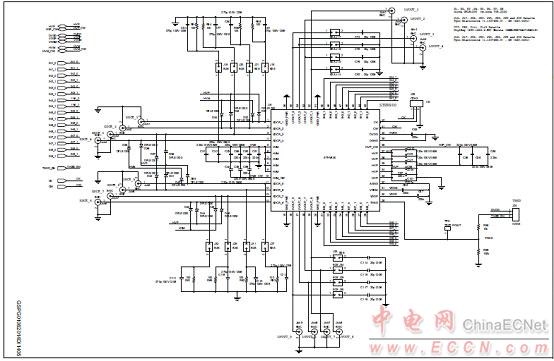
图12.评估板STEVAL-IME009V1电路图(8)
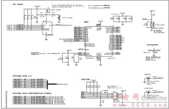
图13.评估板STEVAL-IME009V1电路图(9)
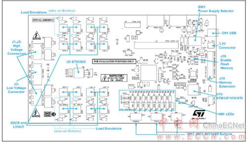
图14.评估板STEVAL-IME009V1 PCB布局图
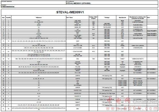
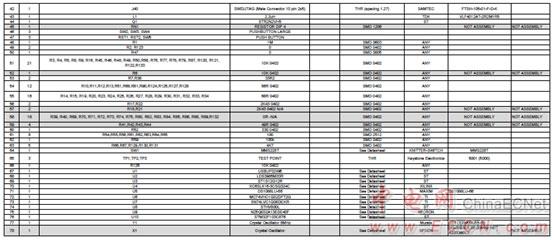
评估板STEVAL-IME009V1材料清单:
Remarkable advances are taking place in medical imaging. Ultrasound imaging helps examine anatomical activity within patients. ST provides with a very wide portfolio of products from discretes to 32 bit digital processors and memories that help to further enhance imaging within ultrasound imaging equipments. The block diagram facilitates your selection among a wide selection of recommended applicable products.

图1.超声波系统框图
The STHV800 is an octal, monolithic, high-voltage and high-speed pulse generator. It is designed for medical ultrasound applications, but can be used for other piezoelectric, capacitive or MEMS transducers.
The device integrates a controller logic interface circuit (compatible with both 1.8 V and 3.3 V input signals), level translators, MOSFET gate drivers, noise blocking diodes, and high power P-channel and N-channel MOSFETs as the output stage for each channel. These MOSFETs are capable of providing more than 2 A of peak output current. Each channel has a dedicated bridge in order to reduce power dissipation and jitter during continuous wave mode (peak current is limited to 0.3 A). This CW bridge has dedicated power supplies (HV_CW) which are fully independent on the main HV supplies.
These HV_CW supplies can be shorted to the HV supplies. The fundamental structure of each channel also consists of active clamping to ground circuitry, anti-leakage and anti-memory block, a thermal sensor to protect the device and an integrated TR-switch (just 8 Ω as equivalent resistor ) to connect the HV output to its LV output, guaranteeing strong decoupling during the transmission phase.
The eight independent T/R switches can be used in both a dedicated RX chain per channel or in a multiplexing configuration.
The clamp circuit has a current capability up to 2 A and works directly on the output pin, carrying this node exactly to zero. This feature allows minimized injection change during the transition from clamp to RX state.
In addition, the STHV800 includes self-biasing circuitry which allows very low power consumption during the RX phase (down to 200 μW global power dissipation) and thermal shutdown block sensing by an external dedicated pin (THSD).
One of the main benefits of this device is that it requires very few external components: only decoupling capacitors on the HV and LV supplies, and a resistor to pull up the THSD pin (moreover, this resistor can be shared by many devices).
Each channel is driven independently by only 2 digital bits, which in CW mode become one bit. An external clock can be used with the STHV800 to synchronize all the input signals. This feature, however, is optional: if the CK pin is tied to ground the device works in asynchronous mode.
STHV800主要特性:
• High-density ultrasound transmitter
• Two independent half-bridges per channel
• 0 to ±90 V output voltage
• Power-up free
• Synchronization of the input signals (selectable) by an external clock
• Up to 20 MHz operating frequency
• Low-power, high-voltage, high-speed drivers
• 2 independently-supplied half bridges (shorted-option) for each channel, one dedicated to continuous wave (CW) mode − Main half bridge: − ±2 A source and sink current
− Down to 20 ps jitter
− Low 2nd harmonic distortion
− CW half bridge: − ±0.3 A source and sink current
− Down to 10 ps jitter
− Very low power consumption
• Fully integrated real clamping-to-ground function − 8 Ω synchronous active clamp
− ±2 A source and sink current
• Fully integrated TR switch − 8 Ω ON resistance
− Up to 300 MHz BW
− Current consumption down to 10 μA in RX phase
− Receiver multiplexing function
• 1.8 V to 3.6 V CMOS logic interface
• Auxiliary integrated circuits − Noise blocking diodes
− Anti-leakage on output node
− Fully self-biasing architecture
− Thermal protection
• Latch-up free due to HV SOI technology
• Very few external passive components or supplies needed
STHV800应用:
• Medical ultrasound imaging
• Pulse waveform generator
• NDT ultrsound transmission
• Piezoelectric transducer drivers
• Point-of-care ultrasound imaging equipment

图2.STHV800内部框图
评估板STEVAL-IME009V1
The STEVAL-IME009V1 is a product evaluation board designed around the STHV800 8-channel high voltage pulser, a state-of-the-art device designed for ultrasound imaging applications.
The output waveforms can be displayed directly on an oscilloscope by connecting the scope probe to the relative BNCs. 16 preset waveforms are available to test the HV pulser under varying conditions.
评估板STEVAL-IME009V1主要特性:
8-channel outputs: high voltage and low voltage BNC connectors
Load simulator using signal equivalent circuits
Possibility to set up own load simulator
16 preset waveforms
USB connector to connect STM32 with PC and supply power to it
4 MB serial Flash memory to host FPGA code and waveforms
Memory expansion connector to add external serial Flash
Connectors to supply high voltage and low voltage to the STHV800 output stage
LEDs to monitor the power management stage
Human machine interface to select, start and stop the generation of the preset waveforms
25 LEDs to monitor board behavior
RoHS compliant

图3.评估板STEVAL-IME009V1外形图

图4.评估板STEVAL-IME009V1硬件框图

图5.评估板STEVAL-IME009V1电路图(1)

图6.评估板STEVAL-IME009V1电路图(2)

图7.评估板STEVAL-IME009V1电路图(3)

图8.评估板STEVAL-IME009V1电路图(4)

图9.评估板STEVAL-IME009V1电路图(5)

图10.评估板STEVAL-IME009V1电路图(6)

图11.评估板STEVAL-IME009V1电路图(7)

图12.评估板STEVAL-IME009V1电路图(8)

图13.评估板STEVAL-IME009V1电路图(9)

图14.评估板STEVAL-IME009V1 PCB布局图
评估板STEVAL-IME009V1材料清单:


|
||||||
|
||||||


