NCP4371高通快速充电3.0协议参考设计
发布时间:2015/10/24 10:03:00 来源:
On Semi公司的NCP4371是次级端充电控制器,支持高通快速充电3.0HVDCP ClassA/B协议,支持充电器USB总线电压根据手机或便携式设备的需求而变化,输出电压从Class A的3.6V到12V,Class B的3.6V到24V,主要用在智能手机,平板电脑和手持设备的快速充电AC/DC适配器.本文介绍了NCP4371主要特性和优势,应用电路,以及15W HVDCP高通快速充电3.0协议参考设计主要特性,指标,电路图,材料清单和PCB设计图.
NCP4371 is a USB secondary side fast-charging controller, supporting Qualcomm Quick Charge™ 3.0 (QC 3.0) High Voltage Dedicated Charging Port (HVDCP) Class A and Class B specification. NCP4371 allows for selection of the output voltage of an AC-DC USB adapter based on commands from the Portable Device (PD) being powered. Selecting a higher charging voltage will reduce the charging current for a given power level resulting in reduced IR drops and increased system efficiency. Another advantage of QC3.0 is a decreased battery charging time and a reduced PD system cost thanks to the ability to select an optimum charging voltage. This eliminates the need for costly DC-DC converters within the PD. The USB-bus voltage can be controlled in discreet steps from 3.6V up to 20V. The output current is limited not to exceed maximum allowable power level.
The NCP4371 resides at the secondary (isolated) side of the adapter. It includes voltage and current feedback regulation eliminating the need for a shunt regulator such as TL431.
The NCP4371 provides charging current limits down to VBUS=2.2V protecting the portable device from excessive currents in case of a soft short-circuit condition.
The NCP4371 integrates a safe-discharge circuitry to quickly and reliably discharge output capacitors in case the USB cable is unplugged or connected to a 5V only USB port.
NCP4371主要特性:
Supports Qualcomm Quick Charge™ 3.0 HVDCP Class A/B
Output Voltage Can be Configured in Discreet Steps from Class A: 3.6V up to 12V Class B: 3.6V up to 20V
Constant Voltage and Constant Current Regulation
Soft Short-Circuit Current Limitation Down to VBUS = 2.2V
USB pins ESD rated to 8 kV
Removes a Need for the Secondary Side Shunt Regulator such as TL431
Output Capacitor Safe-Discharge Circuitry at Cable Unplug
Low Supply Current
Wide Operating Input Voltage Range: 2.2V to 28V
Compatible with USB Battery Charging Specification Revision 1.2 (USB BC1.2)
NCP4371优势:
Increases system efficiency and reduces charging time
Supports a wide range of applications
Provides current protection and system robustness
Provides Short Circuit protection and system robustness
Increased robustness
Reduced BOM
Safety
Increases system efficiency
Design flexibility
NCP4371应用:
Fast Charging AC/DC Adapters for Smart Phones Adapter,Tablets Adapter,Portable Device Adapter
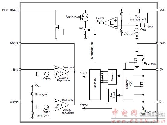
图1.NCP4371框图
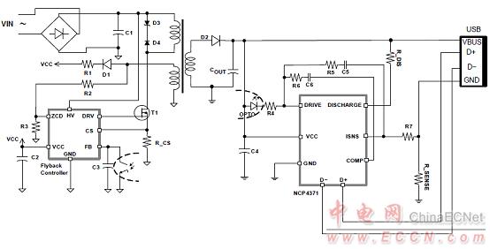
图2.NCP4371框图高通快速充电3.0协议的参考设计
15W HVDCP高通快速充电3.0协议参考设计
This design note describes a 15 W, universal AC mains, isolated Quasi-Resonant flybackconverter compatible with Qualcomm’s High Voltage Dedicated Charging Port Quick Charge™ 3.0 Class A specification. The converter provides adjustable output voltage in a range from 3.6 Vdc to 12 Vdc. It maintains maximum output power 15 W at full range of the voltage output and at same time it limits the maximum output current to 2.0 A. The design is targeted for smart phone and tablet charger applications.
The charger design utilizes ON Semiconductor’s new NCP4371 Qualcomm Quick Charge™ 3.0 Controller, NCP1361E Quasi-Resonant Controller and NCP4305 Synchronous Rectification controller.
高通快速充电3.0协议参考设计主要特性:
Universal AC input range (90 – 265 Vac).
Input filter for conducted EMI attenuation.
Very low standby and no-load power consumption.
Quasi-Resonant current mode control with Valley Switching
Valley lockout avoids audible noise at valley jumping operation
Secondary synchronous rectification control for high efficiency
Qualcomm protocol controller supports QC2.0 and QC3.0
Output 5 V / 2.00 A, 9 V / 1.67 A and 12 V / 1.25 A
Highly configurable power and current limit profiles
Standby power <75 mW @ 5 V output
Support output capacitor discharge function while portable device is unplugged or during transition from higher to lower output voltage
Smooth output voltage transition
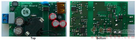
图3. 高通快速充电3.0协议参考设计外形图
高通快速充电3.0协议参考设计主要指标:
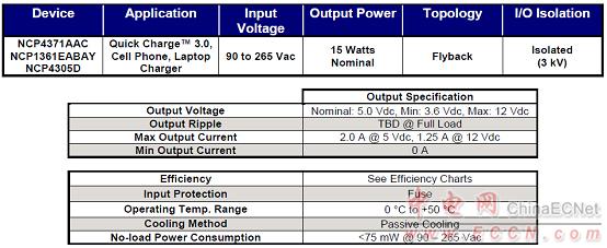
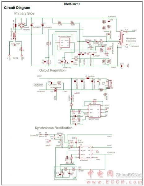
图4.高通快速充电3.0协议参考设计电路
高通快速充电3.0协议参考设计材料清单:
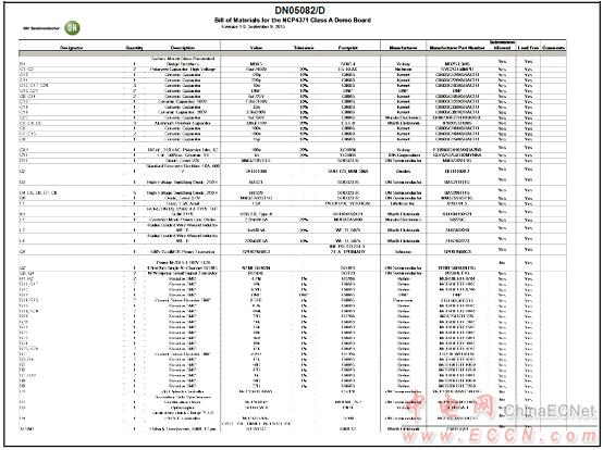
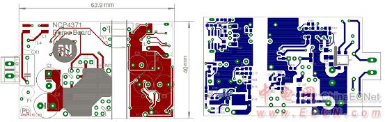
图5.高通快速充电3.0协议参考设计PCB设计图
| |
| |
 |
您可能对以下产品感兴趣 |
 |
|
 |
| 产品型号 |
功能介绍 |
兼容型号 |
封装形式 |
工作电压 |
备注 |
|
| |