当前位置:首 页 --> 方案设计
ADuCM331汽车12V电池系统检测方案
发布时间:2015/9/1 13:00:00 来源:


ADI公司的ADuCM331是用于汽车系统的综合精密电池检测器,集成了8kSPS数据采集系统,包括两个高性能多路sigma-delta (Σ-Δ) ADC,32位ARM Cortex™-M3 MCU和128kB程序闪存和4kB数据闪存,具有检测,处理和诊断功能,是汽车12V电池系统完整的解决方案.本文介绍了ADuCM331优势和特点,框图,典型应用电路图以及评估板EVAL-ADUCM331QSPZ主要特性,电路图和PCB元件布局图.
The ADuCM331 is a fully integrated, 8 kSPS, data acquisition system that incorporate dual, high performance multichannel sigma-delta (Σ-Δ) ADCs, 32-bit ARM Cortex™-M3 processor and flash. The ADuCM331 has 128 kB program flash. and 4 kB data flash. The ADuCM331 is a complete system solution for battery monitoring in 12 V automotive applications. The ADuCM331 integrates all of the required features to precisely and intelligently monitor, process, and diagnose 12 V battery parameters including battery current, voltage, and temperature over a wide range of operating conditions.
Minimizing external system components, the device is powered directly from a 12 V battery. On-chip, low dropout (LDO) regulators generate the supply voltage for two integrated Σ-Δ ADCs. The ADCs precisely measure battery current, voltage, and temperature to characterize the state of the health and the charge of the car battery.
The device operates from an on-chip, 16 MHz high frequency oscillator that supplies the system clock. This clock is routed through a programmable clock divider from which the core clock operating frequency is generated. The device also contains a 32 kHz oscillator for low power operation.
The analog subsystem consists of an ADC with a programmable gain amplifier (PGA) that allows the monitoring of various current and voltage ranges. It also includes a precision reference on-chip. The ADuCM331 integrates a range of on-chip peripherals that can be configured under core software control as required in the application. These peripherals include a SPI serial input/output communication controller, six GPIO pins, one general-purpose timer, a wake-up timer, and a watchdog timer. The ADuCM331 is specifically designed to operate in battery-powered applications where low power operation is critical. The microcontroller core can be configured in normal operating mode, resulting in an overall system current consumption of <18.5 mA when all peripherals are active. The device can also be configured in a number of low power operating modes under direct program control, consuming <100 µA. The ADuCM331 also includes a LIN physical interface for single wire, high voltage communications in automotive environments.
The device operates from an external 3.6 V to 18 V (on VDD, Pin 26) voltage supply and is specified over the −40°C to +115°C temperature range, with additional typical specifications at +125°C.
ADuCM331优势和特点:
High precision analog-to-digital converters (ADCs)
Dual channel, simultaneous sampling I-ADC 20-bit Σ-Δ (minimizes range switching)V/T ADC 20-bit Σ-Δ
Programmable ADC conversion rate from 1 Hz to 8 kHz
On-chip ±5 ppm/°C voltage reference
Current channel Fully differential, buffered input Programmable gain (from 4 to 512) ADC absolute input range: −200 mV to +300 mVDigital comparator with current accumulator feature
Voltage channel Buffered, on-chip attenuator for 12 V battery input
Temperature channel External and on-chip temperature sensor options
Microcontroller
ARM Cortex-M3 32-bit processor
16 MHz precision oscillator with 1% accuracy
Serial wire Debug (SWD) port supporting code download and debug
Automotive qualified integrated local interconnect network (LIN) transceiver LIN 2.2 compatible slave, 100k fast download option
SAE J-2602 compatible slave
Low electromagnetic emissions (EME)
High electromagnetic immunity (EMI)
See data sheet for additional features
ADuCM331应用:
Battery sensing/management for automotive and light mobility vehicles
Lead-acid battery measurement for power supplies in industrial and medical domains.
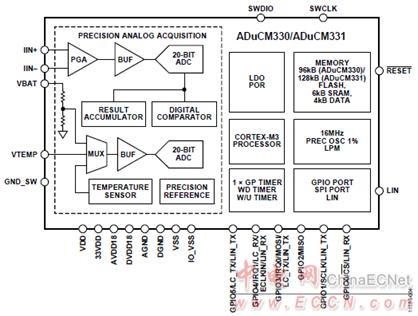
图1.ADuCM331功能框图
图2.ADuCM331典型应用电路图
评估板EVAL-ADUCM331QSPZ
The EVAL-ADUCM331QSPZ development system supports both the ADuCM330 and the ADuCM331 and allows a flexible platform for evaluation of the ADuCM330/ADuCM331 silicon. It allows quick removal and insertion of a device via a 32-lead LFCSP socket. It also provides the connections necessary to allow rapid measurement setups. Switches and LEDs are provided on the applications board to assist in debugging and simple code development. Sample code projects are also provided to show key features of each peripheral and examples of how they can be configured. This user guide provides step-by-step details of how to set up and configure the example software available on the ADuCM33x Design Tools page. By working through this user guide, users can start to generate and download their own user code for use in their own, unique end-system requirements. Full specifications on the ADuCM330/ADuCM331 are available in the product data sheet, which should be consulted in conjunction with this user guide when working with the evaluation board.
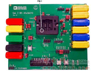
图3.评估板EVAL-ADUCM331QSPZ外形图
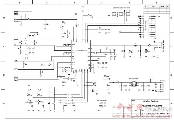
图4.评估板EVAL-ADUCM331QSPZ电路图
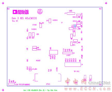
图5.评估板EVAL-ADUCM331QSPZ PCB元件布局图(正面)
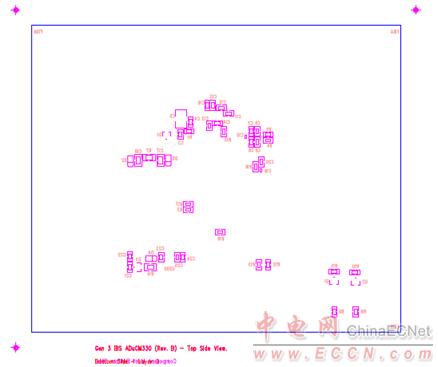
图6.评估板EVAL-ADUCM331QSPZ PCB元件布局图(背面)
The ADuCM331 is a fully integrated, 8 kSPS, data acquisition system that incorporate dual, high performance multichannel sigma-delta (Σ-Δ) ADCs, 32-bit ARM Cortex™-M3 processor and flash. The ADuCM331 has 128 kB program flash. and 4 kB data flash. The ADuCM331 is a complete system solution for battery monitoring in 12 V automotive applications. The ADuCM331 integrates all of the required features to precisely and intelligently monitor, process, and diagnose 12 V battery parameters including battery current, voltage, and temperature over a wide range of operating conditions.
Minimizing external system components, the device is powered directly from a 12 V battery. On-chip, low dropout (LDO) regulators generate the supply voltage for two integrated Σ-Δ ADCs. The ADCs precisely measure battery current, voltage, and temperature to characterize the state of the health and the charge of the car battery.
The device operates from an on-chip, 16 MHz high frequency oscillator that supplies the system clock. This clock is routed through a programmable clock divider from which the core clock operating frequency is generated. The device also contains a 32 kHz oscillator for low power operation.
The analog subsystem consists of an ADC with a programmable gain amplifier (PGA) that allows the monitoring of various current and voltage ranges. It also includes a precision reference on-chip. The ADuCM331 integrates a range of on-chip peripherals that can be configured under core software control as required in the application. These peripherals include a SPI serial input/output communication controller, six GPIO pins, one general-purpose timer, a wake-up timer, and a watchdog timer. The ADuCM331 is specifically designed to operate in battery-powered applications where low power operation is critical. The microcontroller core can be configured in normal operating mode, resulting in an overall system current consumption of <18.5 mA when all peripherals are active. The device can also be configured in a number of low power operating modes under direct program control, consuming <100 µA. The ADuCM331 also includes a LIN physical interface for single wire, high voltage communications in automotive environments.
The device operates from an external 3.6 V to 18 V (on VDD, Pin 26) voltage supply and is specified over the −40°C to +115°C temperature range, with additional typical specifications at +125°C.
ADuCM331优势和特点:
High precision analog-to-digital converters (ADCs)
Dual channel, simultaneous sampling I-ADC 20-bit Σ-Δ (minimizes range switching)V/T ADC 20-bit Σ-Δ
Programmable ADC conversion rate from 1 Hz to 8 kHz
On-chip ±5 ppm/°C voltage reference
Current channel Fully differential, buffered input Programmable gain (from 4 to 512) ADC absolute input range: −200 mV to +300 mVDigital comparator with current accumulator feature
Voltage channel Buffered, on-chip attenuator for 12 V battery input
Temperature channel External and on-chip temperature sensor options
Microcontroller
ARM Cortex-M3 32-bit processor
16 MHz precision oscillator with 1% accuracy
Serial wire Debug (SWD) port supporting code download and debug
Automotive qualified integrated local interconnect network (LIN) transceiver LIN 2.2 compatible slave, 100k fast download option
SAE J-2602 compatible slave
Low electromagnetic emissions (EME)
High electromagnetic immunity (EMI)
See data sheet for additional features
ADuCM331应用:
Battery sensing/management for automotive and light mobility vehicles
Lead-acid battery measurement for power supplies in industrial and medical domains.
图1.ADuCM331功能框图
图2.ADuCM331典型应用电路图
评估板EVAL-ADUCM331QSPZ
The EVAL-ADUCM331QSPZ development system supports both the ADuCM330 and the ADuCM331 and allows a flexible platform for evaluation of the ADuCM330/ADuCM331 silicon. It allows quick removal and insertion of a device via a 32-lead LFCSP socket. It also provides the connections necessary to allow rapid measurement setups. Switches and LEDs are provided on the applications board to assist in debugging and simple code development. Sample code projects are also provided to show key features of each peripheral and examples of how they can be configured. This user guide provides step-by-step details of how to set up and configure the example software available on the ADuCM33x Design Tools page. By working through this user guide, users can start to generate and download their own user code for use in their own, unique end-system requirements. Full specifications on the ADuCM330/ADuCM331 are available in the product data sheet, which should be consulted in conjunction with this user guide when working with the evaluation board.
图3.评估板EVAL-ADUCM331QSPZ外形图
图4.评估板EVAL-ADUCM331QSPZ电路图
图5.评估板EVAL-ADUCM331QSPZ PCB元件布局图(正面)
图6.评估板EVAL-ADUCM331QSPZ PCB元件布局图(背面)
|
||||||
|
||||||