当前位置:首 页 --> 方案设计
AD5676低功耗8通道16位DAC解决方案
发布时间:2015/5/15 9:28:00 来源:
ADI公司的AD5676R是低功耗8通道16位缓冲电压输出数模转换器(DAC),内置2.5V 2 ppm/˚C内部基准电压源和上电复位电路,采用多功能串行外设接口(SPI),时钟速率最高达50 MHz, 工作温度−40℃ 到+125℃,工作电压2.7 V到5.5 V,主要用在光收发器,基站功率放大器,过程控制(可编程逻辑控制[PLC]I/O卡),工业自动化和数据采集系统.本文介绍了AD5672R/AD5676R主要特性,功能框图,菊花链接图以及AD5676R评估板主要特性,框图,电路图和材料清单.
The AD5672R/AD5676R are low power, octal, 12-/16-bit buffered voltage output digital-to-analog converters (DACs). They include a 2.5 V, 2 ppm/℃ internal reference (enabled by default) and a gain select pin giving a full-scale output of 2.5 V (gain = 1) or 5 V (gain = 2). The devices operate from a single 2.7 V to 5.5 V supply and are guaranteed monotonic by design. The AD5672R/AD5676R are available in a 20-lead TSSOP package and incorporate a power-on reset circuit and a RSTSEL pin that ensures that the DAC outputs power up to zero scale or midscale and remain there until a valid write. The AD5672R/AD5676R contain a power-down mode, reducing the current consumption to 1 μA typical while in power-down mode.
AD5672R/AD5676R主要特性:
High performance
High relative accuracy (INL): ±3 LSB maximum at 16 bits
Total unadjusted error (TUE): ±0.14% of FSR maximum
Offset error: ±1.5 mV maximum
Gain error: ±0.06% of FSR maximum
Low drift 2.5 V reference: 2 ppm/℃ typical
Wide operating ranges
−40℃ to +125℃ temperature range
2.7 V to 5.5 V power supply
Easy implementation
User selectable gain of 1 or 2 (GAIN pin)
1.8 V logic compatibility
50 MHz SPI with readback or daisy chain
Robust 2 kV HBM and 1.5 kV FICDM ESD rating
20-lead, TSSOP RoHS-compliant package
AD5672R/AD5676R应用:
Optical transceivers
Base station power amplifiers
Process control (PLC input/output cards)
Industrial automation
Data acquisition systems
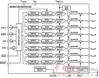
图1. AD5672R/AD5676R功能框图
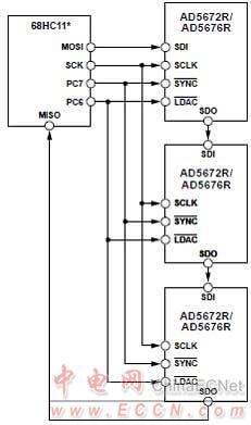
图2. AD5672R/AD5676R菊花链接图
AD5676R评估板EVAL-AD5676SDZ/EVAL-AD5676RSDZ
This user guide details the operation of the evaluation boards for the AD5676/AD5676R octal channel, voltage output digital-to-analog converter (DAC).
The EVAL-AD5676SDZ/EVAL-AD5676RSDZ evaluation boards help users to quickly prototype new AD5676/AD5676R circuits and reduce design time. The AD5676/AD5676R operate from a single 2.7 V to 5.5 V supply. The AD5676R has an internal 2.5 V reference giving a maximum output voltage of 2.5 V or 5 V. The AD5676 does not have an internal reference; therefore, an ADR431 is provided on-board as a 2.5 V reference source. A different reference voltage can be applied via the EXT_REF SMB connector, if required. Full data on the AD5676/AD5676R are available in the respective product data sheets, available from Analog Devices, which should be consulted in conjunction with this user guide when using the evaluation boards.
The evaluation boards interface to the USB port of a PC via the SDP board. Software is supplied with the evaluation board to allow the user to program the AD5676/AD5676R.
The evaluation boards are compatible with the EVAL-SDP-CB1Z Blackfin® SDP controller board (SDP-B), which is available for order on the Analog Devices website at www.analog.com.
评估板EVAL-AD5676SDZ/EVAL-AD5676RSDZ主要特性:
Full featured evaluation board for the AD5676/AD5676R
Various link options
PC control in conjunction with the Analog Devices, Inc., EVAL-SDP-CB1Z system demonstration platform (SDP)
评估板EVAL-AD5676SDZ/EVAL-AD5676RSDZ包括:
EVAL-AD5676SDZ/EVAL-AD5676RSDZ evaluation board
CD includes
Self-installing evaluation software that allows users to control the board and exercise all functions of the device
Electronic version of the EVAL-AD5676SDZ/ EVAL-AD5676RSDZ user guide
ADDITIONAL EQUIPMENT AND SOFTWARE NEEDED
EVAL-SDP-CB1Z SDP board, includes a USB cable
PC running Windows XP SP2, Windows Vista, or Windows 7 with USB 2.0 port
ONLINE RESOURCES
Documents Needed
AD5676/AD5676R data sheet
EVAL-AD5676SDZ/EVAL-AD5676RSDZ user guide
Required Software
AD5676(R) evaluation software (download from the EVAL-AD5676SDZ/EVAL-AD5676RSDZ product pages)
Design and Integration Files
Schematics, layout files, bill of materials
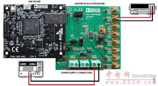
图3. 评估板EVAL-AD5676SDZ/EVAL-AD5676RSDZ建立图
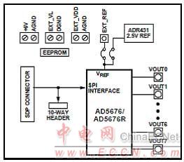
图4. 评估板EVAL-AD5676SDZ/EVAL-AD5676RSDZ框图
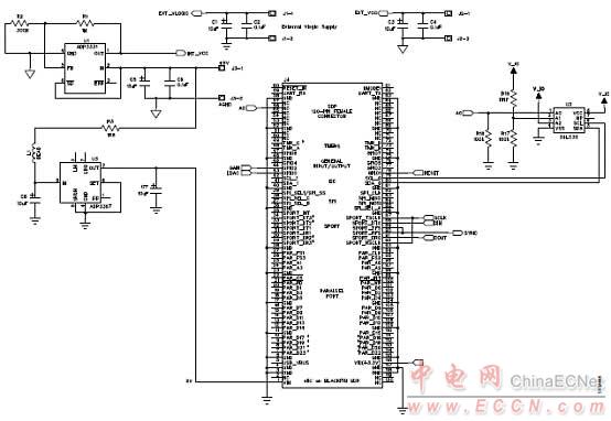
图5. 评估板EVAL-AD5676SDZ/EVAL-AD5676RSDZ电路图(1)
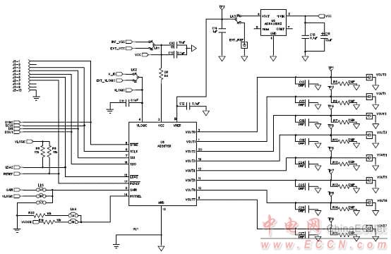
图6. 评估板EVAL-AD5676SDZ/EVAL-AD5676RSDZ电路图(2)
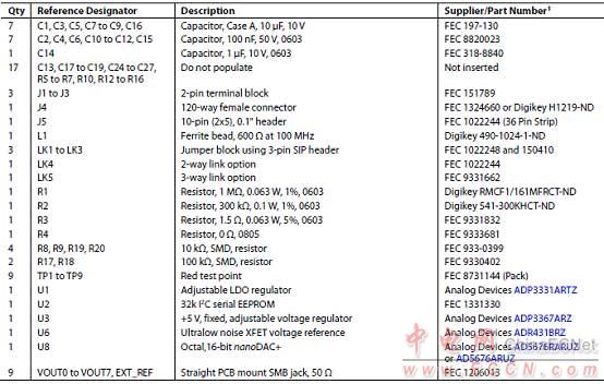
评估板EVAL-AD5676SDZ/EVAL-AD5676RSDZ材料清单:
AD5672R/AD5676R 分别是低功耗、8通道、12/16位缓冲电压输出数模转换器(DAC),内置2.5 V、2 ppm/˚C内部基准电压源(默认使能)和增益选择引脚,满量程输出为2.5 V(增益=1)或5 V(增益=2)。 采用2.7 V至5.5 V单电源供电,通过设计保证单调性。 这些器件采用20引脚TSSOP封装。
AD5672R/AD5676R还内置一个上电复位电路和一个RSTSEL引脚,确保DAC输出上电至零电平或中间电平,直到执行一次有效的写操作为止。 每个器件都具有各通道独立掉电特性,在掉电模式下,器件功耗降至2.5 µA。
AD5672R/AD5676R采用多功能串行外设接口(SPI),时钟速率最高达50 MHz,并均包含一个为1.8 V/3 V/5 V逻辑电平准备的VLOGIC引脚。
产品特色
高相对精度(INL)。
AD5672R(12位):±0.1 LSB(最大值)
AD5676R(16位):±3 LSB(最大值)
低漂移2.5 V片内基准电压源。
The AD5672R/AD5676R are low power, octal, 12-/16-bit buffered voltage output digital-to-analog converters (DACs). They include a 2.5 V, 2 ppm/℃ internal reference (enabled by default) and a gain select pin giving a full-scale output of 2.5 V (gain = 1) or 5 V (gain = 2). The devices operate from a single 2.7 V to 5.5 V supply and are guaranteed monotonic by design. The AD5672R/AD5676R are available in a 20-lead TSSOP package and incorporate a power-on reset circuit and a RSTSEL pin that ensures that the DAC outputs power up to zero scale or midscale and remain there until a valid write. The AD5672R/AD5676R contain a power-down mode, reducing the current consumption to 1 μA typical while in power-down mode.
AD5672R/AD5676R主要特性:
High performance
High relative accuracy (INL): ±3 LSB maximum at 16 bits
Total unadjusted error (TUE): ±0.14% of FSR maximum
Offset error: ±1.5 mV maximum
Gain error: ±0.06% of FSR maximum
Low drift 2.5 V reference: 2 ppm/℃ typical
Wide operating ranges
−40℃ to +125℃ temperature range
2.7 V to 5.5 V power supply
Easy implementation
User selectable gain of 1 or 2 (GAIN pin)
1.8 V logic compatibility
50 MHz SPI with readback or daisy chain
Robust 2 kV HBM and 1.5 kV FICDM ESD rating
20-lead, TSSOP RoHS-compliant package
AD5672R/AD5676R应用:
Optical transceivers
Base station power amplifiers
Process control (PLC input/output cards)
Industrial automation
Data acquisition systems

图1. AD5672R/AD5676R功能框图

图2. AD5672R/AD5676R菊花链接图
AD5676R评估板EVAL-AD5676SDZ/EVAL-AD5676RSDZ
This user guide details the operation of the evaluation boards for the AD5676/AD5676R octal channel, voltage output digital-to-analog converter (DAC).
The EVAL-AD5676SDZ/EVAL-AD5676RSDZ evaluation boards help users to quickly prototype new AD5676/AD5676R circuits and reduce design time. The AD5676/AD5676R operate from a single 2.7 V to 5.5 V supply. The AD5676R has an internal 2.5 V reference giving a maximum output voltage of 2.5 V or 5 V. The AD5676 does not have an internal reference; therefore, an ADR431 is provided on-board as a 2.5 V reference source. A different reference voltage can be applied via the EXT_REF SMB connector, if required. Full data on the AD5676/AD5676R are available in the respective product data sheets, available from Analog Devices, which should be consulted in conjunction with this user guide when using the evaluation boards.
The evaluation boards interface to the USB port of a PC via the SDP board. Software is supplied with the evaluation board to allow the user to program the AD5676/AD5676R.
The evaluation boards are compatible with the EVAL-SDP-CB1Z Blackfin® SDP controller board (SDP-B), which is available for order on the Analog Devices website at www.analog.com.
评估板EVAL-AD5676SDZ/EVAL-AD5676RSDZ主要特性:
Full featured evaluation board for the AD5676/AD5676R
Various link options
PC control in conjunction with the Analog Devices, Inc., EVAL-SDP-CB1Z system demonstration platform (SDP)
评估板EVAL-AD5676SDZ/EVAL-AD5676RSDZ包括:
EVAL-AD5676SDZ/EVAL-AD5676RSDZ evaluation board
CD includes
Self-installing evaluation software that allows users to control the board and exercise all functions of the device
Electronic version of the EVAL-AD5676SDZ/ EVAL-AD5676RSDZ user guide
ADDITIONAL EQUIPMENT AND SOFTWARE NEEDED
EVAL-SDP-CB1Z SDP board, includes a USB cable
PC running Windows XP SP2, Windows Vista, or Windows 7 with USB 2.0 port
ONLINE RESOURCES
Documents Needed
AD5676/AD5676R data sheet
EVAL-AD5676SDZ/EVAL-AD5676RSDZ user guide
Required Software
AD5676(R) evaluation software (download from the EVAL-AD5676SDZ/EVAL-AD5676RSDZ product pages)
Design and Integration Files
Schematics, layout files, bill of materials

图3. 评估板EVAL-AD5676SDZ/EVAL-AD5676RSDZ建立图

图4. 评估板EVAL-AD5676SDZ/EVAL-AD5676RSDZ框图

图5. 评估板EVAL-AD5676SDZ/EVAL-AD5676RSDZ电路图(1)

图6. 评估板EVAL-AD5676SDZ/EVAL-AD5676RSDZ电路图(2)
评估板EVAL-AD5676SDZ/EVAL-AD5676RSDZ材料清单:

AD5672R/AD5676R 分别是低功耗、8通道、12/16位缓冲电压输出数模转换器(DAC),内置2.5 V、2 ppm/˚C内部基准电压源(默认使能)和增益选择引脚,满量程输出为2.5 V(增益=1)或5 V(增益=2)。 采用2.7 V至5.5 V单电源供电,通过设计保证单调性。 这些器件采用20引脚TSSOP封装。
AD5672R/AD5676R还内置一个上电复位电路和一个RSTSEL引脚,确保DAC输出上电至零电平或中间电平,直到执行一次有效的写操作为止。 每个器件都具有各通道独立掉电特性,在掉电模式下,器件功耗降至2.5 µA。
AD5672R/AD5676R采用多功能串行外设接口(SPI),时钟速率最高达50 MHz,并均包含一个为1.8 V/3 V/5 V逻辑电平准备的VLOGIC引脚。
产品特色
高相对精度(INL)。
AD5672R(12位):±0.1 LSB(最大值)
AD5676R(16位):±3 LSB(最大值)
低漂移2.5 V片内基准电压源。
|
||||||
|
||||||


